Article Content
1 Introduction
Plasmonic nanoparticles (NPs) have attracted significant research interest over many years thanks to their wide range of applications, such as photocatalysis, tumor therapy, sensing, bio-imaging, and optical data storage [1,2,3,4]. The incorporation of plasmonic NPs into a dielectric host material allows for tailoring its optical response, potentially achieving exceptional properties that could not be found in nature. The optical response of metal-dielectric nanocomposites can be controlled either by the NPs themselves or by arranging them into plasmonic/ photonic structures. When metallic NPs interact with incident light, the collective electrons on the surface oscillate, a phenomenon known as localized surface plasmon resonance (LSPR), which determines the optical response of the system. It has been demonstrated that LSPR depends on the size, shape, orientation of the NPs, and the surrounding medium [5,6,7]. Although this dependence can tailor the spectral response of the material, fabricating NPs with a high symmetry control is challenging, often resulting in broad distributions of size, shape, and orientation, which lead to weak SPR [8]. In contrast, an interesting approach is proposed by arranging metal NPs into lattices [9,10,11] or assembling them into stable 2D or 3D clusters [12,13,14]. In such configurations, the optical response of the system can be tuned over a wide range by adjusting the lattice period or the interparticle distance. This method offers an effective efficient way to control optical properties compared to tuning the characteristics of individual NPs.
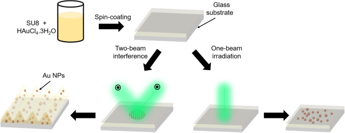
Schematic representation of the fabrication process using one-beam and two-beam interference techniques. The interference is realized by two laser beams having the same polarizations perpendicular to the incident plane, as indicated by dots surrounding by rings
For the fabrication of plasmonic nanoparticle gratings (PNG), bottom-up techniques are the most efficient method, as they arrange metallic NPs into periodic structures. Direct laser writing (DLW) has emerged as a promising method for synthesizing metal NPs as well as PNGs. In this method, the reduction of the metal precursor occurs under light irradiation, via photo-reduction or thermal-reduction mechanism [15,16,17,18], followed by the aggregation process to form NPs. The DLW technique allows the fabrication of 1D, 2D, and even 3D nanocomposite metal/dielectric structures, offering promising applications in metamaterials, color printing, data storage, and bio sensor. Although DLW is a powerful and versatile technique, it has the drawback of requiring complex and expensive equipment. Additionally, the DLW process is time-consuming, as each structure must be fabricated step-by-step, and the fabrication area is extremely limited, typically on the scale of hundred micrometers. To fabricate NPs and PNGs over a large area in a convenient time, alternative methods are required.
Previously, we demonstrated that plasmonic NPs can be directly fabricated within a polymer matrix over a large area using a thermal treatment method [19]. The hybrid metal complex/photoresist sample was placed on a hot plate at an appropriate temperature, facilitating the simultaneous evaporation of the solvent and the polymerization of SU-8. The mechanism of Au NP formation differs from those reported in previous works [10, 15,16,17], which primarily rely on a photo-reduction mechanism. In our approach, the formation of plasmonic NPs begins with a purely thermal reduction of metal complexes into atoms at a suitable temperature, followed by solvent evaporation, which facilitates the nucleation process and leads to the formation of Au NPs.
In another work concerning the direct fabrication of plasmonic structure by using a dewetting method, we had demonstrated that an optically induced thermal effect [20] can do a similar or even better work than that realized in a hot plate. The thermal effect was observed by using an extended continuous-wave (CW) beam, where the material absorbs the light and locally induces a thermal effect. This has been recently employed to produce desired polymeric structures containing Au NPs [18]. However, the structure is small and the fabrication time is quite long.
In this work, we propose a fast technique allowing realization of large polymeric structures containing Au NPs. We first investigate the formation of Au NPs in a large area by irradiating the hybrid gold precursor/photoresist sample using one large CW laser beam. We then propose to apply a two-beam interference technique as a simple and efficient method to arrange the NPs into periodic plasmonic structures, and to further study the formation of Au NPs in various conditions. Diverse types of periodic structures are then realized, offering significant potential for applications in the fields of plasmonics and nanophotonics.
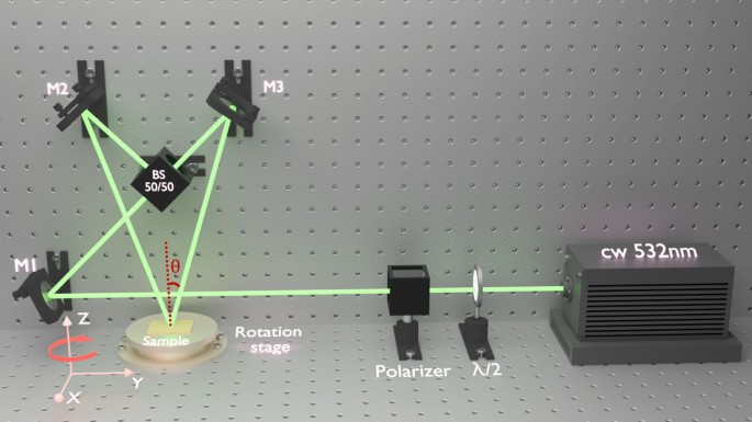
Two-beam interference setup. : Half-wave plate, BS: Non-polarizing beam spliter, M (i=1, 2, 3): Metallic mirrors
2 Experimental methods
2.1 Sample preparation
Gold(III) chloride trihydrate (HAuCl3HO) was purchased from Sigma-Aldrich. SU-8 2000.5 (epoxy-based negative photoresist) was purchased from MicroChem Corporation. The procedure for fabricating PNG, as shown in Fig. 1(a), involves three steps: (i) Gold precursor was mixed with SU-8 resist at different weight ratios (wt) by stirring for 15 minutes for complete dissolution. (ii) The hybrid gold precursor/resist solution was then deposited on a glass substrate by spin-coating at 500 rpm for 5 s, followed by 2000 rpm for 30 s. Since the deposited film is colorless, it indicates that there are no NPs at this stage. (iii) Subsequently, one large beam or a two-beam interference lithography was performed to create and arrange Au NPs, resulting in the formation of PNG. The fabricated structures can be first observed by optical microscope (OM) and atomic force microscope (AFM), and optical diffraction measurements. To obtain more information about the Au NPs embedded in the polymer, we replaced the glass substrate by carbon grids, which allow for transmission electron microscopy (TEM) analysis.
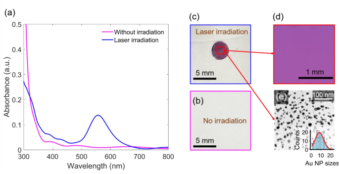
Result obtained with a single laser beam. (a) Absorption spectrum of a hybrid 5wt HAuCl3HO/SU-8 resist, obtained with and without laser irradiation. (b) and (c) Optical microscope images of the sample, showing the cases with and without exposure, respectively. (d) Zoom-in images of the red square region in (c). (e) TEM image of corresponding sample. The excited laser is a CW laser with a wavelength of 532 nm and a power of 500 mW. The irradiation time is 10 minutes
2.2 Experimental setup
The experimental setup for both single large-beam irradiation and the two-beam interference lithography is illustrated in Fig. 2. We use a CW laser operating at a wavelength of 532 nm as the excitation source. A combination of a half-wave plate (/2) and a polarizer allows us to control the laser power. The polarizer is oriented so that the polarizations of two interfering beams are the same at the sample position. This polarization is named S-polarization, which is perpendicular to the incident plane, as indicated by dots surrounding by rings in Fig. 1. After passing through a 50/50 beam splitter, the two beams have identical spatial profiles, polarization and intensities. We note that to study the polarization dependence on PNG formation, another /2 or a quarter-wave plate (/4) was added just after the polarizer (not shown).
The beam has a diameter of approximately 5 mm, with an average power of 70 mW for each beam. The two beams are then redirected by mirrors to interfere with each other, creating a one-dimensional (1D) intensity on the sample area. The half-angle between the two laser beams, denoted by as shown in Fig. 2, can be easily adjusted using a pair of control mirrors. The period of the interference pattern is determined by the angle and the laser wavelength , as given by the following formula:
3 Results and discussion
3.1 Fabrication of Au NPs in a large area by using a single laser beam
Figure 3 shows the results obtained by using a large collimated laser beam on the hybrid sample. Without laser exposure, the sample remains colorless, with its absorption primarily dominated by the gold precursor, which shows strong absorption in the ultraviolet region. However, when the sample is exposed to the laser for 15 minutes (laser power of 500 mW, and laser beam diameter of about 4 mm), the irradiated area turns purple, as shown in Fig. 3(c), indicating the formation of Au NPs. As explained before, under laser irradiation, the thermal reduction changes metal complexes into atoms and accelerates the evaporation of the SU-8 solvent, which drives the reduced Au atoms together, leading to the formation of Au NPs. At this stage, the absorbance in the UV region decreases, and the plasmonic peak of the Au NPs emerges at 560 nm. Figure 3(e) shows the TEM analysis, indicating that this method produces small NPs predominantly around 10 nm in size. Due to the LSPR of Au NPs, the induced temperature increases, triggering the polymerization process of SU-8 resist, which locks the Au NPs in solid SU-8 resist film. These results demonstrate that with one collimated laser beam, we can fabricate Au NPs over a large area. However, the Au NPs were grown randomly within the SU-8 resist. To organize Au NPs into ordered plasmonic structures, it is necessary to modulate the thermal effect, which can be achieved by the high-intensity modulation offered by the interference technique.
3.2 Fabrication of plasmonic structures by using two-beam interference technique
Two-beam interference lithography emerges as a highly promising and cost-effective technique, allowing the fabrication of nano/micro structures simultaneously over a large area during a single exposure [21].
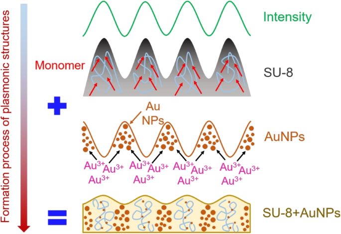
The mechanism of PNG formation using the two-beam interference technique
Figure 4(b) illustrates the formation mechanism of PNG by applying a two-beam interference technique. Under the illumination of an interference pattern, in the constructive interference regions where the highest intensity occurs, the optically induced thermal effect generates radicals that initiate polymerization. This reduces the concentration of SU-8 monomers, driving a net flux of monomers into that region [22], leading to the formation of surface relief gratings (SRG) of SU-8 resist. At the same time, this thermal effect reduces the gold precursor to atoms and facilitates the evaporation of the solvent in SU-8, which pushes the Au atoms together to form Au NPs. As SU-8 monomers migrate into the constructive interference region, Au NPs are pushed toward the regions of destructive interference [23, 24]. When exposure duration is sufficient, even in low light-intensity zones, the plasmonic effect due to the presence of Au NPs within these domains allows them to strongly absorb light and convert it into heat, raising the temperature of the material. At this stage, the SU-8 monomers in the destructive interference regions begin to polymerize, which stabilizes Au NPs and prevents further aggregation in those areas. This mechanism of PNG formation is thus different from previous work [10], where Au NPs were formed only in the constructive regions.
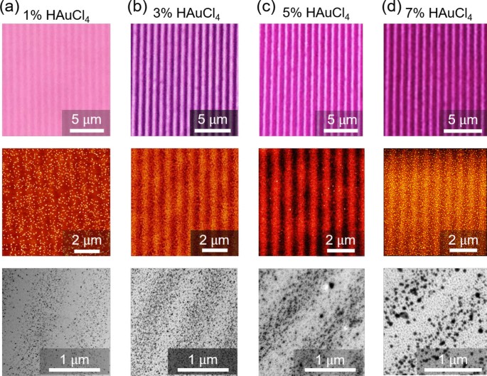
Optical microscope, atomic force microscope, and transmission electron microscope images of the 1D interference pattern at different gold precursor concentrations are shown in the first, second, and third rows, respectively, with the period of 1 m ( = 15.43, = 532 nm)
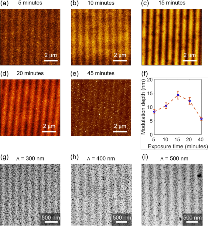
(a)-(e) Fabrication of 1D PNG with a period of 1 m when the irradiation time increases from 5 to 45 minutes. (f) Modulation depth of the grating as a function of exposure time. A 10 error bar was added to represent the uncertainty in the experimental measurement. (g)-(i) Fabrication of the 1D grating with the small achievable period of 300, 400, and 500 nm, respectively. The concentration of gold precursor is 5 wt
3.2.1 Dependence on Au precursor concentrations
We first investigated the influence of varying concentrations of the gold precursor on the formation of PNG. SU-8 was mixed with different ratios of the gold precursor, ranging from 1 to 7 wt, and then irradiated with the interference pattern for 10 minutes. Figure 5 shows corresponding experimental results. The first row displays optical microscope images of the fabricated 1D periodic structures, where the purple color indicates the formation of Au NPs. The structure ( = 1 m, consistent with the result calculated from (1) using an angle of = 15.43) is quite regular over a large area. The bright fringes, where constructive interference occurs, are the region where SU-8 was polymerized, with very few Au NPs formed in this area. In contrast, the darker fringes, where destructive interference occurs, contains a higher concentration of Au NPs. To observe the morphology of the structures, AFM measurements are realized, as shown in the second row. It was observed that, for the same irradiation time, the sample with 5 wt gold precursor shows the best sinusoidal surface gratings, featuring the highest modulation contrast and a depth of around 15 nm. This sample also performed the best in diffraction measurements, though it is not illustrated here. In contrast, the other hybrid sample displayed significantly lower grating depths, varying below 10 nm, resulting in poor contrast when observing the structures. Since AFM only probes the Au NPs located at the surface of the sample, we also performed TEM analysis to obtain information about the NPs embedded within the polymer, as illustrated in the third row. The NPs are roughly spherical in shape, and it is clear that as the concentration of the gold precursor increases, the size of the Au NPs in the destructive fringe grows as well, from 10 nm (1 wt) to 80 nm (7 wt). In fact, a higher quantity of gold precursor leads to the formation of more Au NPs, which is easier to aggregate to form larger particles. In contrast, in the constructive interference region, smaller Au NPs are formed, with this effect becoming more pronounced when the gold concentration exceeds 3 wt, and the particles appear quite uniform at a gold concentration of 7 wt. We expected that if the concentration of the gold precursor is higher than 10 wt, a continuous metallic line may be formed like those obtained by two-photon absorption based DLW [15]. However, when trying with such a high concentration, the interference method did not produce any clear periodic structure but likewise a random Au NPs distribution in solid SU-8 resist. Additionally, the dependence of the SRG on the polarization of the irradiation laser was also tested, but no effect was observed. This is because the process is primarily driven by the thermal effect, which is minimally influenced by changes in polarization. In contrast, for other types of polymers, such as azopolymers (typically DR1/PMMA), the molecules are highly sensitive to polarization, resulting in changes to surface modulation during exposure under different polarization states [25]. Therefore, the polarization state of excitation beams is maintained at S-polarization for all fabrications. We note that, at present, our method creates mostly spherical Au NPs. However, various anisotropic shapes, such as hexagonal, triangular, square, or rectangular can be achieved by mixing Au precursors with other polymers, such as polymethyl methacrylate (PMMA) or polyvinyl alcohol (PVA) [26, 27] in a uniform thin film. The formation of Au NPs in SU-8 resist with anisotropic shapes in periodic structures are more challenging and is under investigation.
3.2.2 Dependence on exposure time
Another factor that affects the formation of PNG is the irradiation time. Figures 6(a)-(e) show the AFM images of the fabricated 1D gratings, with irradiation times increasing from 5 to 45 minutes. It is clear that the grating depth increases from 5 minutes, reaching its maximum at 15 minutes, and then decreases as the hybrid sample is exposed for longer durations. Actually, as the irradiation time increases, monomers migrate towards regions of higher intensity (constructive interference) and accumulate, leading to an increase in grating depth. Meanwhile, the reduced Au ions form Au NPs in this area and move to regions of lower intensity (destructive interference), where they accumulate, creating a Au NPs grating. This process causes a reduction in polymer grating modulation after prolonged irradiation, as shown in Fig. 4. By optimizing the fabrication parameters, we can achieve 1D grating with small periods of 300 nm, 400 nm, and 500 nm. We note that with such small periods, no SRG have been observed by either OM or AFM, only TEM allowed us to observe the organization of Au NPs, as shown in Figs. 6(g)-(i). These periodic structures show great potential for applications, such as plasmonic-based color printing [8, 28].
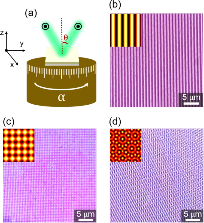
(a) Multi-exposure two-beam interference setup for the fabrication of 1D and 2D periodic structures. (b) One exposure with = 0. (c) Two exposures with = 0 and 90, respectively. (d) Six exposures with = 0, 30, 60, 90, 120, and 150. The period of all structures is 1 m. The inset shows the theoretical calculation of the interference pattern, based on the multi-exposure two-beam interference method
3.2.3 Fabrication of 2D periodic structures by multiple exposures
Two-beam interference lithography also allowed the fabrication of 2D and 3D nano/micro structures [21]. To fabricate 2D periodic structures, we rotate the hybrid sample around the axis by an angle of for multiple exposures. Figure 7(a) shows a schematic of the multi-exposure two-beam interference lithography setup. The sample is placed in the interference area and mounted on a rotation stage. Before fabrication, theoretical calculations of multi-exposure two-beam interference are performed to predict the fabricated structures, based on previous work [21, 29, 30]. Figures 7(b)-(d) show the fabrication and corresponding simulation results of different periodic and quasi-periodic structures. Without rotating the sample, 1D structure (Fig. 7(b)) is fabricated in a single exposure. By irradiating the sample two or multiple times with different angles, 2D structures can be fabricated. For example, Fig. 7(c) shows a 2D square structure fabricated by two exposures at = 0 and = 90. 2D quasi-periodic structure was also fabricated using six exposures at = 0, 30, 60, 90, 120, and 150, as shown in Fig. 7(d). The 1D and 2D structures fabricated in this work were created on an SU-8 2000.5 film with a thickness of 500 nm. We also expect that it could be realized using a thicker SU-8 film (SU-8 2005 or SU-8 2025) to obtain 3D plasmonic/photonic structures by introducing an additional degree of freedom—rotating the sample around the axis [21]. Another method, such as multi-beam interference, where multiple beams (three or more) are simultaneously interfered [31,32,33], is also proposed as a way to fabricate 3D plasmonic/photonic structures. In these cases, the solvent content will be different, and the fabrication parameters should be thoroughly re-optimized.
4 Conclusion
In this work, we have demonstrated a simple and efficient method using a multi-exposure two-beam interference technique to fabricate Au NP gratings within a polymer thin film over a large area. In the constructive region, the monomers begin to cross-link and polymerize, while the high intensity simultaneously induces a thermal effect that facilitates the solvent evaporation process of the polymer, leading to the formation of Au particles that move to the destructive area. Different plasmonic 1D gratings were obtained, with periodicity as small as 300 nm, showing high uniformity over large areas. The highest modulation depth achieved under optimal conditions: (i) a gold precursor concentration of 5 wt; and (ii) irradiation time of 10-15 minutes. By applying multiple exposures, various configurations of 2D periodic structures, such as square and quasi-patterns, are fabricated based on the number of exposures and the rotation angle of the sample for each exposure. The experimental results are consistent with the simulations using the theory for multi-exposure of two-beam interference. This technique proves to be highly effective for the fabrication of nano/micro plasmonic/photonic structures.