Article Content
1 Introduction
Lead monoxide (PbO) exists in various stoichiometries, and studies have shown that the lead-to-oxygen ratio significantly affects its band gap [1]. At environmental conditions (ambient temperature and pressure), there are two stable forms of Pb(II)O: litharge and massicot [2]. Litharge is obtained by heating lead in the atmosphere or an oxygen environment up to about 600 °C. Litharge represents the crystal form of PbO that appears at lower temperatures; it is red and has a tetragonal structure. Massicot represents the higher temperature phase of PbO; it is yellow and has an orthorhombic chain structure. The relative phase stability of litharge (PbOtet) and massicot (PbOorth) is highly sensitive to impurities [3,4,5]. Lead monoxide has long been a preferred metal oxide structure in many fields. In the future, PbO, which can be used as a valuable industrial material in various industries, shows potential applications in passivation layers, rechargeable lithium-ion batteries, valve-regulated lead-acid batteries, and reversible polymer solar cells. Additionally, it can function as a surface modification layer and a photoactive layer in Schottky-type photovoltaic systems [6]. It is a critical industrial material used in a wide range of applications such as gas sensors, pigments, and paints. This material has a wide band gap and contains two polymorphic forms: red α-PbO, stable at low temperatures, and yellow β-PbO, stable at high temperatures. Due to its application diversity, significant advancements have been made in the synthesis of lead (II) monoxide polymorphs (α-PbO and β-PbO) over the years [7, 8]. The main goal in the analysis of metal oxide (such as PbO) nanostructures is the detailed examination of their chemical and physical properties, the development of products with superior characteristics, and the improvement of production processes to create more durable, lightweight products and ensure energy savings. The reactivity of nanoparticles varies based on their size, shape, surface composition, and surface atomic arrangement [9].
Thin films, which are fundamental to electronic device technologies and part of nanotechnology, have a significant place among current research and studies. The performance provided by thin films, which have a very wide range of applications, is a key parameter. The achieved performance is directly related to the type of material used and various production techniques. Differences in production techniques not only give thin films superior properties but also pave the way for new studies. With technological advancements, alternative production techniques have been developed for thin film production. These production techniques have particularly advanced with the advent of vacuum systems. Compared to conventional techniques, modern thin film preparation methods such as CBD and SILAR offer advantages such as cost-effectiveness, ease of process control, lower temperature requirements, and higher uniformity [10]. SILAR and CBD are particularly favored for their simplicity, scalability, and ability to produce films with precise control over thickness and morphology, making them well-suited for large-scale manufacturing processes [11]. These advantages make them highly suitable for large-scale industrial applications and enable enhanced material properties such as improved crystallinity, better adhesion, and enhanced optoelectronic characteristics. Both methods have shown to be more cost-effective than other thin film deposition techniques such as sputtering and pulsed laser deposition, particularly in terms of material utilization and energy efficiency [12, 13]. The extensive use of thin films in device technology has led to significant academic studies aimed at reducing costs and increasing performance. CBD, in particular, allows for uniform film deposition at low temperatures and can be applied to various substrates without the need for vacuum systems, making it a highly versatile and economical option. The importance of thin films as a research area is demonstrated by the growing number of scientific studies conducted worldwide [14].
Various methods for the production of lead oxide (PbO) have been examined and evaluated in different scientific studies. Among these methods are techniques such as spray pyrolysis [15,16,17,18,19], precipitation or co-precipitation [20,21,22,23], sol–gel [24, 25], SILAR [26, 27], CBD [28], Reactive DC Magnetron Sputtering [29], and vacuum thermal deposition [30, 31] Additionally, Ultrasonic Chemical Bath Deposition provides precise control of nanostructures and is an effective method for producing supercapacitor electrodes. This technique offers innovative solutions in energy storage applications [32, 33]. However, the devices required for these methods, their impracticalities, and their lack of cost-effectiveness search for alternative methods is quite natural. CBD and SILAR stand out due to their simplicity and low cost, and they also avoid the need for high energy consumption and complex setups typically required by other deposition techniques. Among these techniques, CBD and SILAR stand out due to their simple setup, cost efficiency, and the ability to produce high-quality thin films with tailored properties. Studies have shown that SILAR films, compared to those produced by spray pyrolysis or sputtering, exhibit superior uniformity, homogeneity, and better-controlled morphology. These methods have shown significant potential in producing PbO thin films with controlled morphology, grain size, and enhanced optoelectronic properties, making them superior to conventional deposition methods [34, 35]. Economical methods for thin film production involve processes that result in an aqueous solution through a chemical reaction. In this context, CBD and SILAR are the most commonly used techniques. These methods only require knowledge of the chemical process involved.
In our study, the two most effective methods for the production of PbO thin films, which hold a significant position in metal oxide materials science, namely CBD and SILAR, are examined in detail. By comparing the structural, morphological, and optical properties of the thin films produced by these two methods, we aim to determine which method would be more efficient for future studies. Furthermore, the electrical and interface properties of Al/PbO/p-Si/Al Metal–Oxide–Semiconductor (MOS) type diodes produced by both methods are analyzed in detail under dark and illuminated conditions, focusing on important parameters such as current–voltage (I–V), differential resistance (Rj), and interface state density (Nss), to obtain valuable insights.
2 Experimental
2.1 The materials and the preparation stages
At the beginning of our research, we focused on the physical and chemical cleaning of glass substrates and silicon crystals. The glass substrates were subjected to a cleaning process to remove chemical and physical contaminants using a solution containing 10% hydrofluoric acid (HF). After the cleaning process, the glass substrates were rinsed thoroughly with deionized water. The rinsing process was carried out in an ultrasonic bath, and the substrates were then carefully dried. To prepare Al/PbO/p-Si Schottky diodes, we used p-type Si (silicon) crystals that were crystallized in the (100) direction, with a doping concentration of 1 × 1015 cm−3, a thickness of 400 µm, and a resistivity of 1-10Ω.cm. Similar cleaning procedures were applied to the silicon crystals.
2.2 Preparation of PbO thin film by SILAR method
PbO thin films were obtained on glass substrates using the SILAR method with two different solutions prepared in distilled water, namely 0.1 M lead acetate trihydrate (Pb (CH3COO)2 · 3H2O) and 2% hydrogen peroxide (H2O2). High-purity (Pb (CH3COO)2 · 3H2O) salt from Sigma-Aldrich was dissolved in 50 mL of DI water to initiate the process. The prepared 0.1 M solution was stirred with a magnetic stirrer for 10 min. Then, 5 mL of ammonium hydroxide (NH4OH) and 5 mL of triethylamine [(C2H5)3N] (TEA) were added to the solution and stirred continuously for 1 h. TEA functions as a complexing agent, stabilizing lead ions in the precursor solution and regulating the film growth rate. Its presence enhances film uniformity and adhesion preventing uncontrolled precipitation. Using 5 ml of triethylamine has been determined as the optimal condition based on experimental optimization. This volume ensures the high quality of the films by preventing issues related to excessive or insufficient complexation. Additionally, it helps control the pH of the solution, facilitating the desired development of film morphology, crystallinity, and electro-physical properties. Generally, the effect of variations in thin film formation depends on factors such as the method used, temperature, pH, and film thickness. These parameters influence the crystalline structure, morphology, optical, and electrical properties of the thin films [36]. This solution served as the cationic source for thin film formation. In the second beaker, a 2% H2O2 solution was prepared and used as the anionic source for PbO thin film. The pH value of the anion precursor solution was measured to be approximately 8, while the pH value of the cation precursor solution was approximately 11. After the preparation of the solutions, all materials were placed in an 80 °C heater. When the temperatures of all solutions and deionized water were equalized, the coating process was carried out without changing the temperature throughout the coating duration.
The SILAR method for PbO thin film deposition involves a cyclic immersion process. Figure 1 shows the schematic representations of PbO thin film by SILAR. First, the glass substrate is submerged in a lead ion precursor solution, enabling the adsorption of lead complex ions onto the surface. Following this adsorption step, the substrate is rinsed with deionized (DI) water to remove loosely bound lead ions. Next, immersion in a hydrogen peroxide (H2O2) solution promotes a reaction between the lead complex ions and H2O2, forming PbO. A final rinse step with DI water removes any weakly bound PbO species. This cycle is repeated for a specified number of times (e.g., 15 cycles) to achieve the desired film thickness. Finally, an annealing step at elevated temperatures (e.g., 350 °C for 30 min) helps remove residual hydroxide phases.
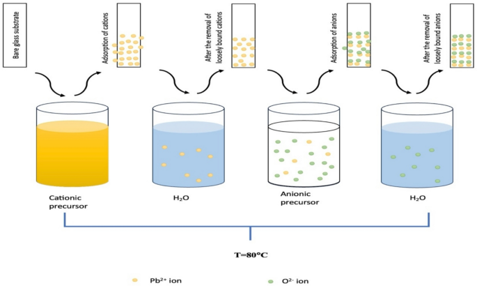
Schematic representations of PbO thin film by SILAR method
2.3 Preparation of PbO thin film by CBD method
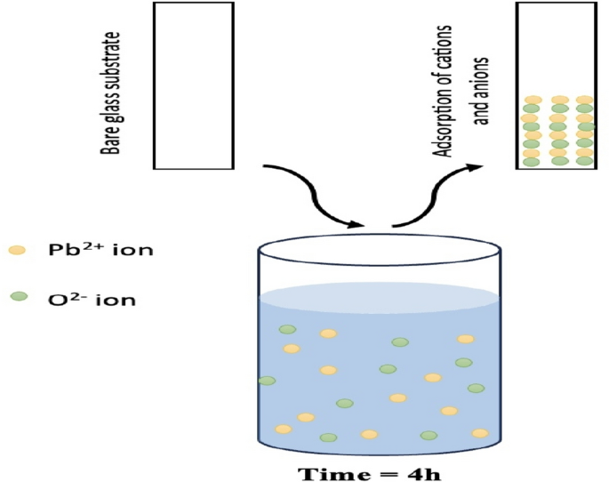
The solution prepared for SILAR, which was discussed in detail in the previous section, was prepared with the same steps and in the same way for the chemical bath. The cleaned glass substrates, which underwent both chemical and physical cleaning, were placed into the prepared solution and left at room temperature for 4 h. Figure 2 shows the steps. Subsequently, the resulting thin film was annealed at 350 °C for 30 min.
Schematic representations of PbO thin film by CBD method
2.4 Preparation of Al/PbO/p-Si diodes via SILAR and CBD
The same p-Si crystals with the mentioned properties were initially subjected to traditional chemical cleaning procedures for both coating methods. Subsequently, a high-purity Al metal was deposited onto the matte surface of the crystals using a PVD system to create ohmic contacts. For ohmic contact formation, the crystals were annealed in a nitrogen gas environment at 570 °C for 3 min. Then, similar to the process applied on glass, the shiny surface of the p-Si/Al substrate was coated with a PbO thin film using the SILAR deposition method for 15 cycles. To prevent undesired conditions, the matte surface was cleaned using cotton after every 5 cycles. The procedure applied on glass in the CBD method was carried out similarly. Here, instead of glass, the crystal was left in the solution for 4 h, and then the matte surface was cleaned with cotton.
After the coating process, films produced by both methods were annealed in a furnace at 350 °C under normal atmospheric conditions for 30 min. Following the formation of the PbO thin film, a thin layer of Al was deposited onto the PbO-coated surface of the substrate by evaporating highly pure Al metal using a vacuum system and a tungsten filament. Thus, Al/PbO/p-Si/Al MOS diodes were successfully obtained by SILAR and CBD methods.
3 Results and discussion
3.1 Microstructural and morphological analysis
Determining the microstructural features and morphological evolutions in PbO thin films prepared with chemical bath and SILAR techniques is very important in discussing the usability of these materials in technological applications. Therefore, microstructural phase determination and properties of the produced thin films were investigated by X-Ray Diffractometer (XRD) and Scanning Electron Microscopy (SEM). Figure 3 shows the X-ray diffraction results of PbO thin films prepared by chemical bath and SILAR techniques. As seen in Fig. 3, XRD results show that diffraction peaks belonging to tetragonal α-PbO (JCPDS card no: 99-101-2269), orthorhombic β-PbO (JCPDS card no: 38-1477) and tetragonal β-PbO2 (JCPDS card no: 76–0564) crystalline phases are formed. Additionally, some parametric values such as d-spacing, (hkl) plane and full width at half maximum (FWHM) obtained from XRD results are given in Table 1. As seen in Fig. 3a-b, in the XRD diffraction patterns of PbO thin films produced by the CBD and SILAR methods, the α-PbO peak intensities are higher and sharper in the CBD method, while they are smaller and the peak width is larger in the SILAR method. Also, as seen in Table 1, the orientations in the α-PbO diffraction peaks formed at approximately the same diffraction angles are in the same plane. However, the FWHM and d-spacing values are usually larger in the SILAR method. These results show that the α-PbO crystals are more dominant and have a more regular structure in the CBD method than in the SILAR method. As seen in Fig. 3a, PbO thin films produced by the chemical bath method have a polycrystalline structure, mostly a tetragonal structure with α-PbO and a little orthorhombic structure with β-PbO. However, as seen in Fig. 3b, the PbO thin film produced by the SILAR method has only a tetragonal polycrystalline structure including α-PbO and β-PbO2 phases. Here, the XRD pattern of β-PbO2 is in good agreement with those reported by Fan et al. [37]. Zhao et al. [38] also observed that β-PbO2 thin film produced through the electrodeposition method shows similar results in XRD studies. In this study, the reason for the appearance of orthorhombic phase (β-PbO) traces at 2θ = 30.863° and 2θ = 59.548° may be due to the substrate temperature adopted in the chemical bath method applied to form the PbO film. The formation of the orthorhombic phase strongly confirms that the crystal structures of PbO thin films transform from α-PbO to β-PbO at 350 °C and higher temperatures. Zhang et al. [39] reported that the α-PbO crystal phase transforms to the β-PbO crystal phase under atmospheric pressure at 490 °C. Moreover, in thin films produced at 400 °C, Panturotai et al. [40] reported that the orthorhombic (β-PbO) dominant peak was clearly observed at 2θ = 30.66°, corresponding to the (020) plane. In a similar study, Suganya et al. [41] also reported that the β-PbO peak occurs at 2θ = 30.863°, corresponding to the (200) plane. As a result, the very sharp formation of the XRD peaks of both α-PbO crystal phases and β-PbO2 crystal phases, where the β-PbO2 crystal phase ratio was calculated as approximately 17% using the Rietveld method, indicates good crystallization and reduced amorphization in the thin film produced by SILAR method.
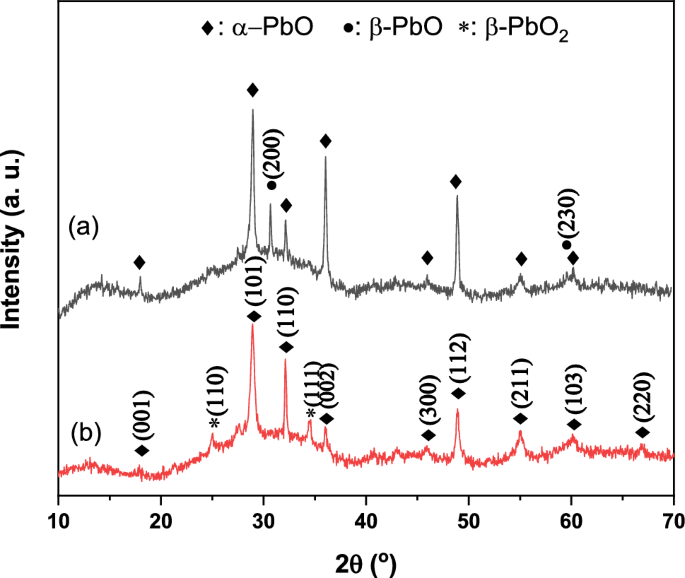
XRD results of produced PbO thin films, a Chemical bath method (CBD), b SILAR method
The Scherrer equation,, to calculate the crystallite size (D) is used, and also the Stokes-Wilson formulas, and , to calculate the lattice strain (ε) and dislocation density (δ), respectively, in the produced PbO thin film are used. For the crystallite size (D) and the lattice strain (ε) equations, λ is the X-ray wavelength (CuKα, 1.5406 Å), β (rad) is the FWHM, and θ is the X-ray diffraction angle. In the calculation with the Scherrer and Stokes-Wilson formulas [42,43,44,45,46], the peak values, which are given in Table 1, obtained in the XRD analysis of the PbO thin films were used, and the calculated average values were given in Table 2. As seen in Table 2, the average crystallite size of the phases formed in the PbO thin film produced by the chemical bath method is larger than the average crystallite size of the phases formed in the PbO thin film produced by the SILAR method. The formation of the PbO2 crystal phase in the PbO thin film produced by the SILAR method caused the average crystallite size to decrease, and the lattice strain and dislocation density to increase. The crystallite size (D) of the PbO2 crystal phase occurred at 2θ = 34.592° was calculated as 29.19 nm, which is in agreement with the literature [47]. Additionally, the results about the crystallite size appear to be consistent with the results reported in previous studies [48, 49]. Furthermore, the crystallite size and lattice strain parameters for PbO thin films are also determined by applying the Williamson–Hall method [12, 50, 51]. The calculated values are given in Table 2. It is seen in Table 2 that the crystallite size and lattice strain values obtained in the SILAR method are larger than those obtained in the CBD method. It is also seen that the same parameter values are smaller than those calculated by the Scherrer method. Consequently, as seen in the XRD results, while the β-PbO phase did not form in the thin film produced with the SILAR method, the formation of the β-PbO2 phase caused the SILAR method to create a smaller crystallite size than the CBD method. Crystal size can be controlled through synthesis parameters and production methods. Factors such as pH, ionic strength, and precursor concentration in solution directly affect crystal growth [52]. Additionally, production techniques such as ultrasonic chemical bath deposition (UCBD) effectively manage crystal size and morphology [32]. Along with UCBD, chemical bath deposition (CBD), successive ionic layer adsorption and reaction (SILAR), vapor phase deposition, spray pyrolysis, and sol–gel methods can also influence the growth rate and orientation of crystals, thereby enhancing material properties. Furthermore, annealing processes alleviate internal stresses in crystals, improving their structural quality. Wang et al. [53] demonstrated that high-temperature annealing enhanced the crystal quality in AlN films. These findings underscore the crucial role of synthesis parameters and production methods in determining crystal size and properties. Also, dislocations, as a common defect in semiconductor crystals, mainly affect the electronic and optical properties of semiconductors. Furthermore, for many crystalline materials, including PbO, the dislocation density typically falls in the range of 1012 m−2 to 1014 m−2.In semiconductor devices, dislocations can serve as effective channels for carrier leakage, leading to a decrease in breakdown voltage. The critical threshold beyond which performance degradation occurs due to dislocation density is a key concept in materials science, particularly in the study of mechanical properties and deformation behavior of crystalline materials. Meanwhile, dislocations are also important scattering factors, and an increase in dislocation density in PbO film with the help of the SILAR method leads to a decrease in electron mobility. Higher dislocation density generally leads to increased electrical resistance due to enhanced electron scattering at the dislocation sites [54,55,56].
Furthermore, the surface morphology of the PbO thin film samples produced by chemical and SILAR methods was investigated by SEM. Figure 4a-b shows the SEM images of the thin films. As seen in Fig. 4a, a tightly bound and porous structure consisting of rod-like or irregular plate-shaped grains was observed for the PbO thin film produced by the chemical bath method. However, the surface of the PbO thin film produced by the SILAR method (Fig. 4b) consists of dense and microspherical-shaped agglomerates. When Fig. 4a and b are compared, smaller hole porosities and smaller grain-size particles are seen in the PbO thin film produced by the SILAR method. As seen in Fig. 4b, spherical-shaped PbO2 particles are smaller in size than PbO particles and are distributed homogeneously in the thin film with a multi-crystalline nanocomposite structure. The existence of PbO and PbO2 crystalline phases in the thin film was also confirmed by EDX analysis. EDX analysis results for Fig. 4a-b are given in Fig. 5a-b. It was observed that EDX values were compatible with XRD analysis results.
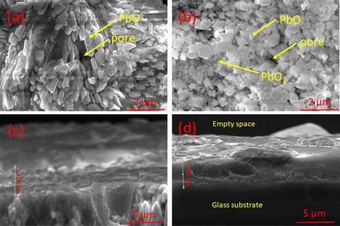
SEM images of produced PbO thin films, a CBD method, b SILAR method, c Cross section of SEM image of Glass/PbO in CBD method, d Cross section of SEM image of Glass/PbO in SILAR method
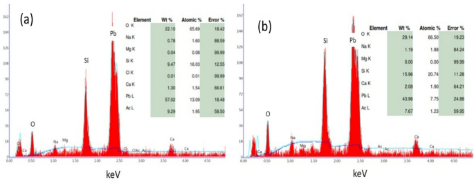
EDX results of produced PbO thin films, a CBD method, b SILAR method
Figure 4c-d presents SEM cross-sectional images showing the thicknesses of PbO thin films produced by CBD and SILAR methods. The thicknesses of PbO thin films were found to be 5.328 μm and 5.096 μm for CBD and SILAR methods, respectively. In the SILAR method, the decrease in film thickness can be associated with decreasing the crystallite size [13, 57, 58] and the amount of PbO crystalline phase.
3.2 Optical measurements of the film (UV–visible)
We believe that the increase in optical transmittance occurs with the growth of crystallites and the decrease in crystallite boundary density. Optical transmittance and absorbance, which are inversely related to each other, are two important properties related to the interaction of light with a material and are commonly used in spectrophotometry to measure the amount of light absorbed by a substance. Analysis of light absorption (optical absorbance spectra) in PbO films deposited using CBD and SILAR techniques was performed across a wavelength range of 200 nm to 1200 nm (as shown in Fig. 6). The results reveal a significant influence of the deposition method on film transparency. Interestingly, both films displayed high transmittance in the visible spectrum and a sharp decrease in absorption (absorption edge) around 350 nm. Films prepared by SILAR exhibited lower overall transmittance, possibly due to factors like film thickness variations, contamination during deposition, differences in oxidation rates, etc. [13, 58, 59].
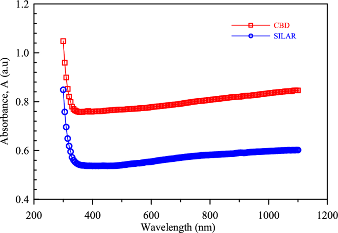
The absorption-wavelength plot of the obtained PbO thin films via CBD and SILAR
It is known that a stoichiometric semiconductor compound, such as lead oxide, exhibits a sharp transmission edge at the photon energy corresponding to its band gap. Assuming only a direct transition between the valence and conduction band edges, the variation of the absorption coefficient with photon energy can be calculated using the following relationship.
In this equation, m is an exponential constant and takes the value ½ in allowed direct transitions. Eg is the optical band gap energy, v is the frequency, h is Planck’s constant, C is the proportionality constant, and A is the absorption coefficient [60]. Figure 7 illustrates the calculation of the optical band gap energy by extrapolating the linear portion of (Ahν)2 vs. hν. The energy band gap values, showing an increasing trend depending on the production technique, are found to be 3.61 eV for CBD and a slightly changed range of 3.75 eV for SILAR. This is consistent with the literature [61, 62]. The larger crystallite size in CBD (42.93 nm) compared to SILAR (35.67 nm) can be associated with decreasing the band gap energy. Crystallite size can profoundly affect the optical behavior of thin films. For example, smaller crystallites can result in larger optical band gaps, altered absorption, and changes in light scattering properties. This is associated with increased surface area-to-volume ratio and higher band gap energy. Yousra et al. [13] reported that UV–visible light transmittance spectra showed that the band gap widened and optical transmittance decreased with increasing film thickness. In this study, the absorption coefficient for SILAR is higher compared to CBD due to less PbO formation and also the formation of the PbO2 crystallite phase, which is advantageous for applications such as solar cells, LDRs and photodetectors. The improvement in light absorption in the SILAR sample compared to CBD is attributed to more reactive free surfaces associated with oxygen vacancies at grain boundaries with the formation of the PbO2 phase.
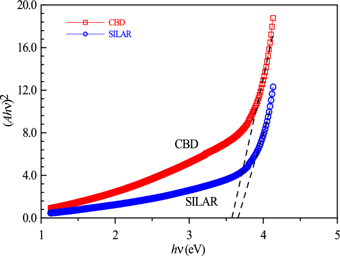
Variation of the obtained film (Ahυ)2 with respect to the photon energy (hυ)
3.3 Current–voltage features of the produced Al/PbO/p-Si diodes
During our experimental investigations, a comparative study was conducted to understand the potential advantages that the PbO interlayer could provide to our work depending on the production method. In this context, the current–voltage data of the Al/PbO/p-Si structure created using both the interlayer-free sample and the CBD, and SILAR methods were measured, and these data were evaluated comparatively. The electrical properties were subjected to a detailed analysis based on the standard thermionic emission theory of the formed structure. This theory considers the carriers that carry the current formed at the junction interface. The current–voltage (I–V) characteristics of the produced Al/PbO/p-Si diodes with a detailed analysis based on the standard thermionic emission theory are presented in Fig. 8.
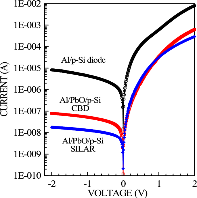
I-V graphs of Al/p-Si reference and Al/PbO/p-Si diode prepared using CBD and SILAR methods in the dark
The current–voltage (I–V) characteristics of the fabricated Al/PbO/p-Si diodes were measured at room temperature and in darkness using a Keithley 4200-SCS apparatus. The I-V relationship can be described by the Shockley equation (Eq. 2):
where I is the current, I0 is the reverse saturation current, VD is the diode voltage, q is the electronic charge, n is the ideality factor, k is the Boltzmann constant, and T is the absolute temperature. Under the assumption that qVD > > nkT, Eq. 2 can be simplified to Eq. 3:
The ideality factor (n) can be determined by taking the derivative of the logarithmic form of Eq. 3 with respect to VD (Eq. 4):
The reverse saturation current (I0) is expressed by Eq. 5:
where, the area of the A diode (A = 0.00785 cm2) is A* Richardson’s constant and its value is A* = 32 AK⁻2 cm⁻2 for p-Si, and ΦB is the Schottky barrier height. Equation 6 allows for the calculation of the Schottky barrier height based on the natural logarithm of both sides of Eq. 5.
Voltage was applied to the diode in the range of − 2 V to + 2 V with increments of 0.02 V, and diode behavior demonstrating rectification characteristics was observed for both CBD and SILAR-produced diodes. Depending on the coating method of the Al/PbO/p-Si Schottky diode, the ideality factor, barrier height, saturation current, and rectification ratios were calculated from the I–V curve graphs. In the I–V graphs, it was observed that the current decreased by approximately 100 times for the diode produced with CBD and by approximately 1000 times for the diode produced with SILAR. This decrease is attributed to an additional resistance effect of the PbO thin film layer between the metal and p-Si and the formation of a natural oxide layer and interface layer at the interface. The approximately tenfold difference in diodes produced with CBD and SILAR can be attributed to film thickness and barrier inhomogeneity formed during production.
In Fig. 8, the barrier height ФB = 0.637 eV and ideality factor n = 1.866 were found for the referenced Al/p-Si diode. The barrier height for the Al/PbO/p-Si diode produced with CBD was calculated as ФB = 0.737 eV with an ideality factor of n = 2.68, while for the diode produced with SILAR, the barrier height was determined as ФB = 0.749 eV with an ideality factor of n = 1.94 (Table 3). SILAR-produced PbO films, with their smoother structure, have fewer defects, enabling better carrier movement, higher Schottky barrier height, and lower ideality factor. In contrast, CBD-produced films, with more defects, exhibit lower Schottky barrier height and higher ideality factor. The crystal structures of PbO films produced by CBD and SILAR affect the transport mechanisms. SILAR produces smoother and more homogeneous films, facilitating the movement of carriers, while CBD films are thicker and rougher, potentially hindering carrier movement. These differences influence the electrical properties of the diodes, and the advantages of each method are evaluated based on application requirements [63].
RS and RSh are parameters that affect the electrical properties of the diodes. These values, calculated using Ohm’s law in forward and reverse bias, are provided from the Rj curves in Fig. 9. The values obtained are respectively RS = 241.6 Ω and RSh = 241.9 kΩ for the reference diode, RS = 3.19 kΩ and RSh = 25.32 MΩ for the diode produced with CBD, and RS = 6.89 kΩ and RSh = 112.40 MΩ for the diode produced with SILAR.
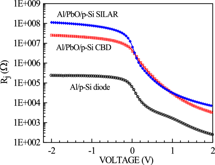
Rj -V graphs of Al/p-Si reference and Al/PbO/p-Si diode prepared using CBD and SILAR methods
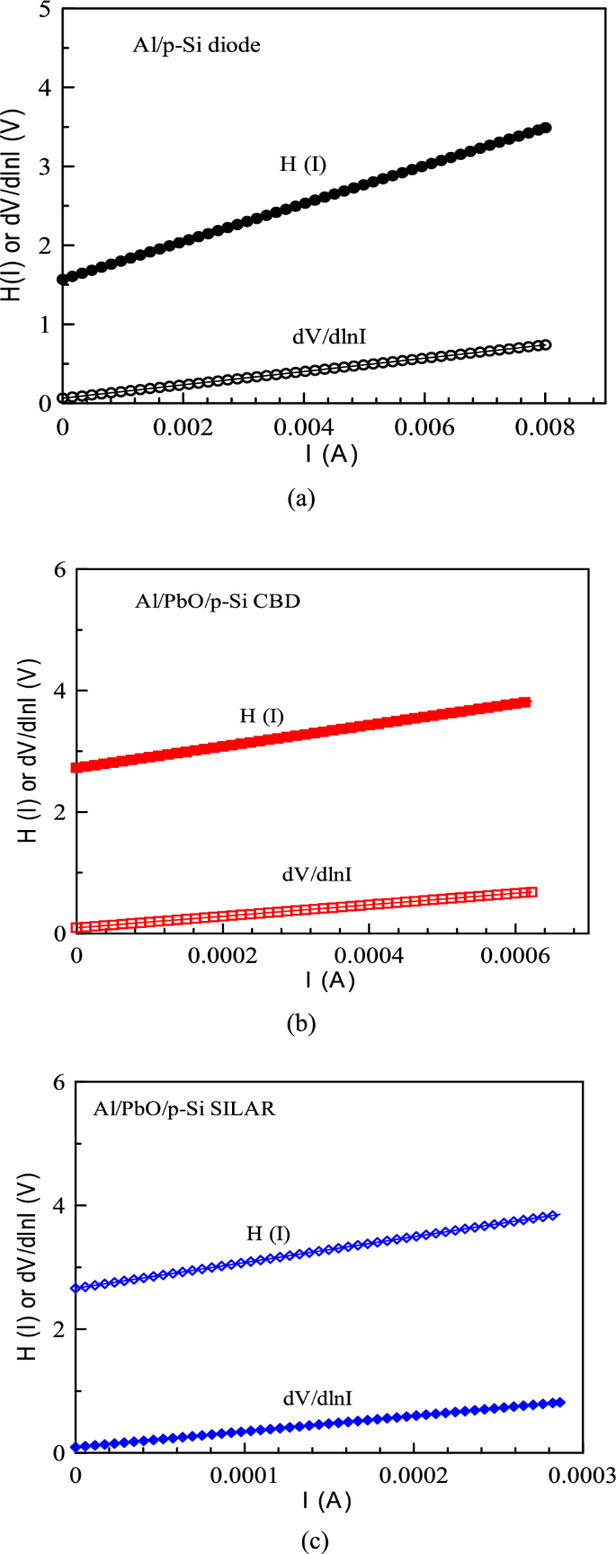
The Cheung method, one of the techniques used to calculate values such as series resistance, barrier height, and ideality factor for the diode, was developed by S.K. Cheung and N.W. Cheung in 1986. The Cheung functions are as follows.
Figure 10 presents the H(I) and dV/d(lnI)-I plots for both Al/PbO/p-Si and Al/p-Si reference diodes fabricated using the CBD and SILAR methods. The linear regions of these plots were used to extract device parameters using the Cheung function. Extracted series resistance (RS) and ideality factor (n) for the Al/p-Si reference diode were RS = 0.0843 kΩ and n = 2.48, respectively. For the CBD-produced Al/PbO/p-Si MOS Schottky diode, the values were RS = 0.945 kΩ and n = 3.57, while for the SILAR-produced diode they were RS = 2.547 kΩ and n = 3.56. Furthermore, the Cheung function applied to the H(I)-I plots yielded the following parameters: For the Al/p-Si reference diode, RS = 240.07 kΩ and barrier height (ΦB) = 0.632 eV. For the CBD-produced Al/PbO/p-Si MOS Schottky diode, RS = 1.764 kΩ and ΦB = 0.763 eV. Finally, for the SILAR-produced diode, RS = 4.175 kΩ and ΦB = 0.748 eV. A summary of these values can be found in Table 3.
H(I) or dV/d(lnI)-V graphs of Al/p-Si reference (a) and Al/PbO/p-Si diode prepared using CBD (b) and SILAR (c) methods
The Norde method is a second method used to calculate important parameters such as barrier height, ideality factor, and series resistance of a diode. This method determines these parameters using the data obtained from the voltage–current (I–V) characteristics of the diode. The Norde functions are the equations primarily used in these calculations. The Norde functions are as follows:
Here, γ is the first integer greater than the ideality factor. I(V) value refers to the current value obtained from the I-V graph.
The ideality factor can be calculated with the following equation (Eq. 11)
The expression for the barrier height calculated by the Norde method:
In this equation, the term F(V0) represents the minimum value of the F-V graph.
The expression for the series resistance is as follows:
Figure 11 presents the F(V)-V plots for both Al/PbO/p-Si and Al/p-Si reference diodes fabricated using the CBD and SILAR methods. From the F(V)-V graphs obtained from Norde functions, the barrier height value for the reference Al/p-Si diode is ФB = 0.652 eV, and the series resistance value is RS = 1.153 kΩ. For the Al/PbO/p-Si diode produced with CBD, the barrier height value is ФB = 0.758 eV, and the series resistance value is RS = 66.559 kΩ. For the diode produced with SILAR, the barrier height value is ФB = 0.777 eV, and the series resistance value is RS = 20.313 kΩ. These values are listed in Table 3.
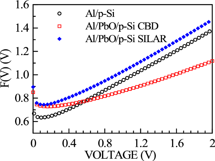
F(V)-V graphs of Al/p-Si reference and Al/PbO/p-Si diode prepared using CBD and SILAR methods
Figure 12 presents the double logarithmic scale Ln(I)-Ln(V) graphs of Al/p-Si, Al/PbO/p-Si (CBD), and Al/PbO/p-Si (SILAR) diodes in the forward bias region. The presence of three distinct linear regions in the graph indicates that the diodes exhibit different conduction mechanisms across various voltage ranges [64, 65]. In the low-voltage region (Region I), the slope values for the Al/p-Si, Al/PbO/p-Si (CBD), and Al/PbO/p-Si (SILAR) diodes were determined as 1.27, 1.22, and 1.37, respectively. These values indicate that the dominant conduction mechanism in the low-voltage region is ohmic conduction. In the intermediate voltage region (Region II), the slope values were found to be 2.21 for the Al/p-Si diode, 2.06 for the Al/PbO/p-Si (CBD) diode, and 2.34 for the Al/PbO/p-Si (SILAR) diode. These results suggest that the conduction mechanism in this region is dominated by the trap-assisted space charge limited current (EDT-SCLC) mechanism. In the high-voltage region (Region III), the slopes were calculated as 3.88 for the Al/p-Si diode, 4.11 for the Al/PbO/p-Si (CBD) diode, and 3.29 for the Al/PbO/p-Si (SILAR) diode. These findings indicate that the space charge limited current (SCLC) mechanism is dominant in the high-voltage region. The presence of the PbO layer and the fabrication method significantly influence the charge transport mechanisms. The CBD-fabricated diodes exhibit higher slope values, indicating a greater density of trap centers. In contrast, the SILAR-fabricated diodes demonstrate lower slope values, suggesting a lower trap density and a more uniform PbO layer. In conclusion, the presence of the PbO layer and the fabrication technique are key factors in determining the electrical characteristics of the diodes in the forward bias region. Optimizing the fabrication process is crucial for enhancing device performance. Additionally, the obtained data are consistent with SEM and XRD results.
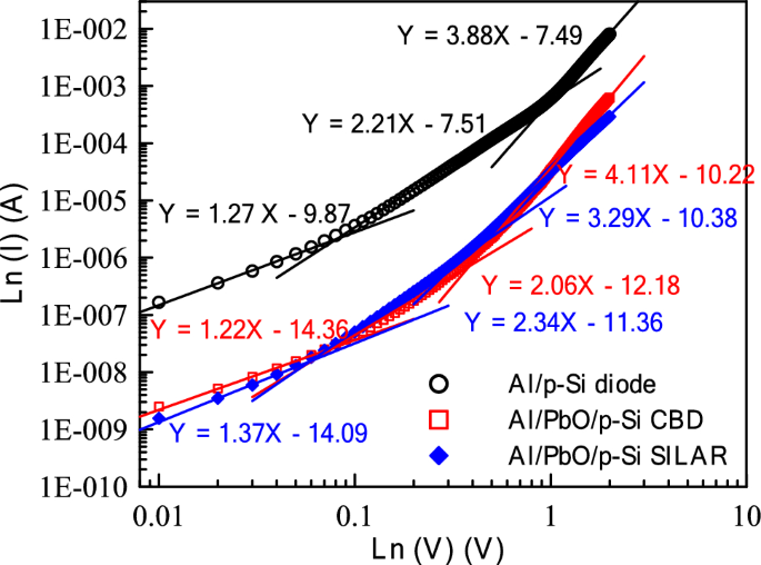
Ln(V) graphs of Al/p-Si, Al/PbO/p-Si (CBD), and Al/PbO/p-Si (SILAR) Schottky Diodes in the forward bias region
3.4 Calculation of interface states
Interface state density (NSS) is a parameter that affects the performance of Schottky diodes. The interface state density of three different diodes produced by CBD, SILAR, and control (Al/p-Si) methods has been calculated using the following equations, utilizing the voltage-dependent profiles obtained from the I-V data.
In the equations, εi represents the dielectric permittivity of the interlayer, δ is the thickness of the interlayer, εs is the semiconductor permittivity, and WD is the depletion region width [66].
As seen in Fig. 13, the NSS values of the diode produced by SILAR become lower than those produced by CBD due to the high dielectric constant. The Nss value decreases with increasing interface layer thickness (WD) and low ideality factor. Barrier height in ideal Schottky contacts arises from the difference between the work functions of the metal and the semiconductor. This scenario assumes the absence of interface states in the ideal Schottky model. However, in real contacts, the presence of interfaces should be considered. These interfaces can arise from factors such as chemical contamination, defects, surface treatments, or surface damage. They lead to deviations from ideality in the diode. Therefore, calculating the interface state density for diodes is important [67].
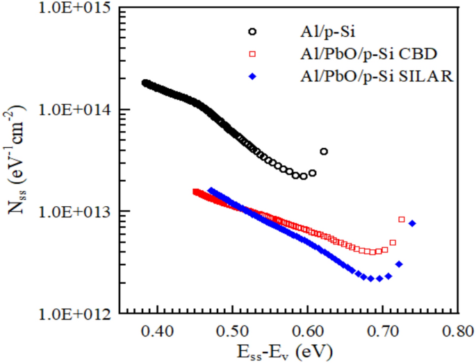
The Nss-(Ess-Ev) graphs of Al/p-Si reference and Al/PbO/p-Si diode prepared using CBD and SILAR methods
3.5 The photodiode characteristics of Al/PbO/p-Si diodes in the illuminated environment
The calculated electronic parameters of the photodiodes provide insights into the diode characteristics. The current–voltage characteristics of the prepared Al/PbO/p-Si diodes were measured under 100 mW/cm2 illumination intensity. As observed in Figs. 14 and 15 below, the reverse bias current of the diode increases significantly when light is applied for both CBD and SILAR-produced diodes. In these graphs, the photodetection sensitivity (Ps), responsivity (R), and detectivity (D*) parameters of both CBD and SILAR-produced Al/PbO/p-Si diodes under 100 mW/cm2 illumination intensity were calculated. These values were compared with the photodetection sensitivity (S), responsivity (R), and detectivity (D*) parameters of circuit elements produced using various metal oxides and organic molecules.
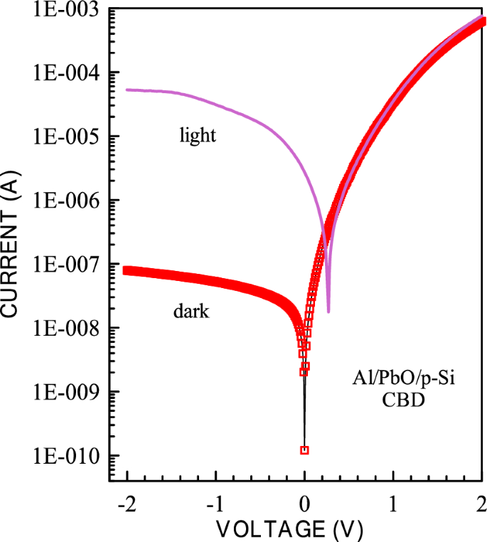
I-V graphs of Al/PbO/p-Si diode prepared using CBD method in the 100 mW/cm2 light intensity
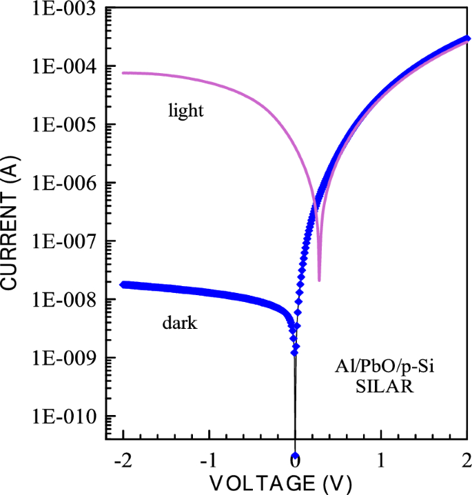
I-V graphs of Al/PbO/p-Si diode prepared using SILAR method in the 100 mW/cm2 light intensity
The photoresponsivity (R) of the diode was determined using the equation (Eq. 17) given below [68]:
where Iph, P, and S are termed as photocurrent, illumination power, and effective area. The values of the Photo responsivity (R) of the Al/PbO/p-Si diode made by CBD and SILAR methods are found to be 66.9 mA/W and 95.9 mA/W at a bias of − 2 V, respectively.
The photosensitivity (PS) of the diode was calculated using the equation (Eq. 18) given below [69]:
The highest photosensitivity at 100 mW/cm2 and − 2 V was found to be 6.65 × 10⁴ and 4.23.105 for the diodes which have made by CBD and SILAR methods, respectively. These values were tabulated in Table 4. Another important parameter is detectivity (D*), which is used to analyze the performance of photodetectors, and is expressed in Eq. 19:
where R, A, Id and q are the responsivity, the active area of the device, the dark current, and the electron charge, respectively. The highest detectivity values at 100 mW/cm2 and − 2 V were found to be 3.72.1010 Jones and 1.13 × 10¹¹ Jones for the diodes which have made by CBD and SILAR methods, respectively. These values were tabulated in Table 4.
R value for p-Si/Fe(II)–polymeric complex/Au diode was found as 3.235 mA/W at -10 V for 100mW/cm2 intensity values of visible light [70]. R and D* values for Au/propolis/n-Si photovoltaic device were found as 12.8 mA/W and 2.17 × 10⁸ Jones at -2 V for 100mW/cm2 intensity values of visible light [71]. The photoresponsivity (R) and specific detectivity (D*) under the illumination intensity of 100 mW/cm2 for In/In2S3/p-Si diode were calculated as 0.192 mAW−1 and 4.83 × 10¹⁰ Jones (Jones = cmHz1/2 W−1), respectively [72]. The photoresponsivity (R) and light sensitivity (Ps) under the illumination intensity of 100 mW/cm2 for Al/ bromothymol blue (BTB)/p-Si diodes were calculated as 0.679 mAW−1 and 1028.85, respectively [73]. The photoresponsivity (R) and light sensitivity (Ps) under the illumination intensity of 100 mW/cm2 for Al/ sunset yellow dye (SY)/p-Si diodes were calculated as 0.101 mAW−1 and 1,028.85, respectively [74]. The values of R and Ps of Au/(CoSO4-PVP)/n-Si diode were found as 101 mA/W and 5.25 × 10³ at − 2 V under 100 mW/cm2 [75].
Our device exhibits a higher photoconductive responsivity under 100 mW/cm2 illumination compared to previously reported GFO/p-Si junctions (responsivity of 5.41 × 10⁻⁵ A/W). This enhanced light sensitivity suggests the fabricated heterojunction has a strong potential for optoelectronic applications like photodiodes and optical sensors [76].
Demirezen et al. found that the photosensitivity (Ps) value was extracted as 1277 for Al/PCBM/NiO:ZnO/p-Si device with 20% NiO content at 100 mW/cm2 [77]. Photodetectors using a Ce-doped V2O5 interface have a peak responsivity of 65.86 mA/W [78], while a La-doped V2O5 interface shows values ranging from 10.33 to 156.21 mA/W [79]. A study with a Ce–WO3 interface recorded a maximum responsivity of 20.61 mA/W [80]. In comparison, the Al/PbO/p-Si photodiode made by the SILAR method exhibits a high responsivity of 95.9 mA/W, indicating its efficiency in light detection. The enhanced photocurrent observed in SILAR-produced diodes can be attributed to the incorporation of the PbO2 phase, which facilitates improved crystallization and mitigates amorphization relative to CBD-produced films. This results in a more ordered crystallographic structure, thereby enhancing carrier mobility and ensuring more efficient charge transport. Additionally, the larger bandgap of PbO2 reduces charge recombination processes, which in turn contributes to the enhanced photodetector performance. Collectively, these factors are responsible for the superior photocurrent and overall performance exhibited by the SILAR-produced diodes.
Surucu et al. [81] reported that the Al/Si3N4/p-Si photodiode has an impressive detectivity (D*) of 3.52 × 10¹⁰ Jones, highlighting its ability to detect low light levels. For context, the Yb-doped V2O5 interface has a detectivity of 9.97 × 10¹⁰ Jones [82], La-doped V2O5 interfaces reach up to 9.82 × 10¹⁰ Jones [79], and Ce-doped V2O5 interfaces have a maximum of 2.99 × 10¹⁰ Jones [78]. The Al/PbO/p-Si photodiode’s detectivity, while lower than these peak values, is still commendable, confirming its effectiveness in applications requiring high sensitivity to low light levels. The Al/PbO/p-Si structure demonstrates promising photo-sensing properties, potentially exceeding those reported in previous studies. This suggests that the photocurrent of the device increases with illumination intensity, possibly due to the generation of a greater number of photogenerated carriers under brighter light.
4 Conclusion
In this study, PbO thin films were successfully prepared using both the CBD and SILAR methods. The microstructural and morphological analyses revealed significant differences between the films produced by these two methods. X-ray Diffraction (XRD) analysis indicated that PbO thin films obtained via the CBD method exhibited a polycrystalline structure, predominantly consisting of tetragonal α-PbO with traces of orthorhombic β-PbO. In contrast, films produced by the SILAR method showed only a tetragonal polycrystalline structure comprising α-PbO and β-PbO2 phases. The formation of β-PbO2 in the SILAR films suggests improved crystallization and reduced amorphization compared to CBD films. The average crystallite size of the SILAR-produced PbO films was smaller than that of CBD-produced films, indicating finer grain sizes in the former. This finer microstructure could positively influence the electrical conductivity by improving charge transport efficiency. Additionally, SEM images revealed distinct surface morphologies, with SILAR films exhibiting denser and more uniform microspherical-shaped agglomerates compared to CBD films. Optical measurements showed that the CBD films had slightly lower optical band gap energies compared to SILAR films, indicating potential advantages for certain optoelectronic applications. The higher absorption coefficient observed in SILAR films, attributed to greater film thickness, enhances light absorption efficiency, which is beneficial for optoelectronic applications. SILAR-produced PbO films, with their smoother structure, have fewer defects, enabling better carrier movement, higher Schottky barrier height, and lower ideality factor. In contrast, CBD-produced films, with more defects, exhibit lower Schottky barrier height and higher ideality factor. The crystal structures of PbO films produced by CBD and SILAR significantly influence the transport mechanisms. SILAR films provide a smoother and more homogeneous morphology, facilitating carrier movement, whereas CBD films exhibit a rougher structure that may hinder efficient charge transport. These differences influence the electrical properties of the diodes, and the advantages of each method are evaluated based on application requirements. Overall, the findings confirm that the SILAR method provides superior microstructural control and enhanced optoelectronic properties compared to the CBD method. However, the choice between these methods should consider specific application requirements and desired film properties. Additionally, the electrical properties and photodiode performance of Al/PbO/p-Si Schottky diodes fabricated via CBD and SILAR methods were investigated. SILAR-produced diodes showed significantly lower current, attributed to PbO and PbO2 layer thickness differences and barrier inhomogeneity. The enhanced photodetector performance in SILAR-produced diodes can be attributed to the higher bandgap of the PbO2 phase and its more ordered crystalline structure. This structure facilitates improved carrier mobility and charge transport efficiency, reducing recombination processes and enhancing overall device performance. Variations in ideality factor, barrier height, and rectification ratios were observed between the two methods. The Cheung and Norde methods provided insights into series resistance and ideality factor calculations, showcasing method-specific differences. Moreover, the space-charge-limited current (SCLC) analysis confirmed that the SILAR method leads to lower trap density and higher carrier mobility, directly contributing to the observed enhancements in diode performance. Additionally, NSS analysis further supported these findings, indicating that SILAR diodes exhibited lower NSS values due to their higher dielectric constants, which contributes to improved charge transport properties. The SCLC results also demonstrated that SILAR-produced films exhibited a more uniform trap distribution, which significantly reduces charge recombination and enhances diode efficiency. Photodiode characteristics, including responsivity, sensitivity, and detectivity, demonstrated the superior performance of SILAR-produced diodes, positioning them as promising candidates for optoelectronic applications. These findings provide a foundation for future research in optimizing PbO thin film fabrication techniques, paving the way for more efficient optoelectronic devices.