Article Content
1 Introduction
To accelerate the advancement of next-generation on-chip communication, there is a growing demand for electro-optical modulators that possess exceptional characteristics such as low-drive voltage, large optical bandwidth, ultra-high speed and compatibility of complementary metal-oxide semiconductor CMOS technologies. The state-of-the-art silicon-photonics technology-based modulators are currently a prime candidate for meeting these requirements (Chaisakul et al. 2019; Reed et al. 2010; Xiao et al. 2023), however they suffer from limited thermal ability, larger foot print, higher energy consumption and insertion loss due to weak plasma dispersion effect. To mitigate the drawbacks of silicon optical modulators, new materials and technology have already been explored. Graphene, a zero-bandgap two-dimensional (2D) material is one of the promising materials that could revolutionize silicon photonics due to its noticeable electrical, mechanical, thermal and optical properties (Bao and Loh 2012; Bonaccorso et al. 2010; Falkovsky 2008; Hendry et al. 2010; Lukosius et al. 2024). Graphene demonstrated an excellent optical property with an ultra-high carrier mobility, wide operational bandwidth, and the ability to tune conductivity electrically. An atomically thinned single layers graphene absorbs 2.3% of the perpendicularly incident light which further can be enhanced by integrating graphene on hybrid waveguide structures (Liu et al. 2011). The absorption of graphene can be tuned by actively tuning the Fermi level through applying voltages. These nailing optical properties of graphene have made it a major contender in various optoelectronics applications including high-speed photodetectors (Schall et al. 2014; Xia et al. 2009), optical polarizers (Bao et al. 2011) and electro-optical modulators (Li et al. 2014; Liu et al. 2012; Romagnoli et al. 2018). In the past few years, different kinds of graphene-based waveguide-coupled optical modulators with single-layer graphene (SLG) and double-layer graphene (DLG) have been studied and demonstrated, based on graphene-oxide-silicon and graphene-oxide-graphene configuration respectively. To date, graphene-based electro-optic modulators with DLG architecture have already shown promising characteristics such as broadband optical bandwidth (Liu et al. 2011), high-speed operation (Giambra et al. 2019; Koester and Li 2012), considerable modulation efficiency (Liu et al. 2012), and larger temperature stability (Dalir et al. 2016). For instance, a DLG based EA optical modulator was proposed in 2012 with a modulation depth of 0.10 dB/µm at modulating voltage 5 V, however the modulation bandwidth was limited to 1 GHz (Li et al. 2014). In 2016, a graphene-based broadband modulator with a modulation depth of 2 dB and high bandwidth of 35 GHz demonstrated (Dalir et al. 2016). However, a large 30 V modulating voltage needed to operate the device to achieve such high bandwidth. Recently, a DLG EA optical modulator was demonstrated with 39 GHz modulation bandwidth and 2.2 dB/V modulation efficiency at moderate drive voltage (Agarwal et al. 2021). However, a 2D–3D hetero-integration of dielectric materials between the two graphene layers are required to achieve such performance. Nevertheless, it should be emphasized that most of the previously reported graphene-based EA optical modulators are based on the silicon-on-insulator (SOI) integrated waveguide. However, the propagation loss of SOI waveguide is relatively large (about 2 dB/cm to 3 dB/cm) due to the surface roughness of silicon stripe. In comparison to SOI waveguides, silicon nitride (Si3N4) waveguide has much lower propagation loss of 0.1 dB/cm. The utilizing of Si3N4 waveguides also offers several advantages such as lower refractive index, broader wavelength transparency windows, reduced thermal-optic effects, and increased fabrication tolerance (Shao et al. 2016). Therefore, in the last few years, Si3N4 waveguide -on- SiO2 platform has gained attention for realizing photonic integrated circuits (PICs) (Lee et al. 2021; Lukose et al. 2023; Phare et al. 2015).
Despite having above mentioned properties of Si3N4 waveguide -on- SiO2 platform, only few graphene-based Si3N4 waveguide-coupled EA optical modulators have been proposed and demonstrated (Lee et al. 2021; Phare et al. 2015). In these reports, graphene EA optical modulators on the Si3N4 platform employ mainly aluminum oxide (Al2O3) or a 2D–3D material based heterostructures as spacer layer between two graphene layers. On one hand, Al2O3, may be used in device concepts where its higher dielectric constant provides benefits, but the increased optical losses must be considered, whereas the complexity and scalability of 2D-3D heterostructures should also be addressed. On the other hand, Si3N4 is as an alternative dielectric spacer which has a much lower absorption coefficient in the near-infrared range, making it a better choice for minimizing optical losses and enhancing the efficiency of graphene-based modulators. It is also a material with higher dielectric strength compared to Al2O3, enabling it to withstand stronger electric field without breakdown. Si3N4 also offers superior insulating properties, resulting in lower leakage currents compared to Al2O3. Additionally, it preserves the high mobility and low doping of intrinsic graphene, enables to operate beyond the transparency regime ensuring superior dynamic performance. Furthermore, Si3N4 exhibits strong thermal stability, making it capable of withstanding high-temperature processing and CMOS compatible. To the best of our knowledge, no reports have yet demonstrated graphene-based modulators integrating Si3N4 as a waveguide as well as a spacer layer between the graphene, highlighting for further exploration and development in this area.
In this paper, an ultra-high-speed and highly efficient buried waveguide-coupled DLG EA optical modulator on Si3N4 platform using a fabrication wise simpler approach has been designed and simulated where the waveguide material and the dielectric spacer between the two graphene layers are Si3N4. This approach not only enhance the graphene-light interaction but also amplifies the capacitance of the EA optical modulators while maintaining their resilience against high voltages. The impact of graphene quality and the waveguide configuration on the modulation efficiency and bandwidth are investigated by finite element method. Subsequently, the dielectric spacer layer thickness between the two graphene layers and graphene size are carefully designed based on the optimized waveguide structure to enhance the modulator’s performance. According to the simulation results, the proposed modulator demonstrated a modulation efficiency of 1.1 dB/V and a modulation depth of 0.16 dB/µm equivalent to an extinction ratio up to 15dB. The proposed modulator achieves a high modulation bandwidth of 14 GHz and operates over a 1050 nm broadband operation spectral range. This research showcases the potential of the proposed design in achieving high-performance electro-optic graphene modulators integrated within Si3N4 waveguides platform.
2 Device structure and modelling
2.1 Device concept
Figure 1 illustrates the schematic structure of the proposed double-layer graphene EA optical modulator. The proposed graphene EA optical modulator comprises a dual-layer graphene capacitor integrated with a Si3N4 waveguide buried on a 2.1 µm-thick buried oxide (BOX: SiO2) layer. The capacitor consists of two graphene sheets (Bottom: GRAP1 and Top: GRAP2) separated by a 20 nm Si3N4 dielectric spacer. The capacitor is enclosed by another 20 nm Si3N4 following by a 1.5 µm silica (SiO2) on the top it as a top cladding (TOX) layer. The Si3N4 dielectric spacer between the two graphene layers plays a crucial role in determining the overall performance (trade-off between modulation efficiency and bandwidth) of the modulator. Therefore, to optimize the modulator’s performance, we conducted a design exploration and optimization for different Si3N4 dielectric spacer thicknesses (), specifically 10 nm, 20 nm, and 30 nm. Efficient metallic contact can be achieved with two Palladium/Gold (Pd/Au) pads positioned on each side of the graphene to electrically tune the graphene electro-optical properties. Both materials offer exceptional thermal and electrical conductivity, coupled with low contact resistance and strong adhesion properties, rendering it ideal choices for contacting graphene. we designed the gap between the waveguide and each metal electrode/pad about 1.5 µm in order to avoid any optical interference between them. The operational principle of our proposed modulator is very straightforward: applying a voltage to the graphene electrodes induces simultaneous electron doping in one electrode and electron depletion in the other. This process leads to a shift in the Fermi energy (chemical potential) and consequently brings about changes in the refractive index and absorption of the waveguide material within the capacitor region.
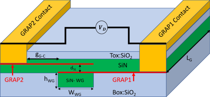
Proposed device schematic : waveguide height : waveguide width, : spacer layer thickness between two graphene, : waveguide to electrode distance and : length of the graphene
2.2 Modelling methodology
The simulations in this work are conducted using the finite difference eigenmode (FDE) solver, while the properties of graphene are described using a surface conductivity model (Hanson 2008). The complex surface conductivity of a monolayer graphene can be obtained through the application of the Kubo formula (Hanson 2008).
where ω is the radian frequency of incident light, μ is the chemical potential that can be electro-statically controlled, is the scattering rate which is inversely proportional to scattering time , is the temperature, is the energy, is the reduced Plank’s constant, is the charge of an electron and is the Fermi–Dirac distribution function:
where the Boltzmann’s constant. The first term in Eq. (1) represents the conductivity contribution arising from intra-band electron-photon scattering process, while the second term is due to inter-band scattering. The permittivity of the graphene can be calculated as a function of the complex conductivity of graphene using a volumetric method (Shao et al. 2016).
where is the permittivity of the air medium and is the thickness of the single layer graphene respectively. Figure 2 shows the simulated conductivity and permittivity of a single layer graphene as a function of graphene chemical potential. The following calculations are based on the incident light with λ, and for three different scattering time τ, e.g. 13 fs, 65 fs and 100 fs that corresponds to graphene mobility of 293, 1466 and 2200 cm2V−1 s−1 at μ respectively (Romagnoli et al. 2018). The scattering time directly impacts the material mobility, which, in turn, plays a crucial role in determining the material’s quality and, consequently, the modulator performance.
Figure 2a illustrates the graphene optical surface conductivity normalized by , the universal graphene conductivity and Fig. 2b illustrate the dielectric permittivity for different τ concerning the Fermi level of a graphene mono-layer, determined using Eq. (1) and Eq. (3) respectively. As the chemical potential () increases, the real part of the permittivity, which primarily governs the material’s refractive properties, gradually rises until it reaches a maximum point when the Pauli blocking condition is met . Afterwards, it experiences a sharp decrease as the increases, it is noteworthy that the sign of the real part of the permittivity constant can transition from positive to negative. This shift implies that the properties of graphene can be altered from dielectric-like to metallic-like characteristics (Giambra et al. 2019). The imaginary part of the permittivity is mainly associated with material absorption and exhibits distinct characteristics depending on the chemical potential. For below the Pauli blocking threshold , a constant region is observed, where inter-band electron-photon scattering dominates. As the approaches the Pauli blocking energy threshold, both inter-band and intra-band processes become significant, leading to a notable change in the imaginary part of the permittivity. Finally, at above the Pauli blocking energy , the imaginary part of the permittivity remains nearly constant and is primarily influenced by the intra-band scattering process. Additionally, the variation in complex permittivity demonstrates elevated values for τ=65 fs and τ=100 fs, owing to their associated higher mobility. In contrast, the change is relatively lower for τ=13 fs due to its correspondingly lower mobility. These findings suggest that higher mobility corresponds to a somewhat superior material quality in comparison to lower mobility. The changes of graphene’s permittivity influence the complex effective mode index (η) in the waveguides and consequently the modulators performance.
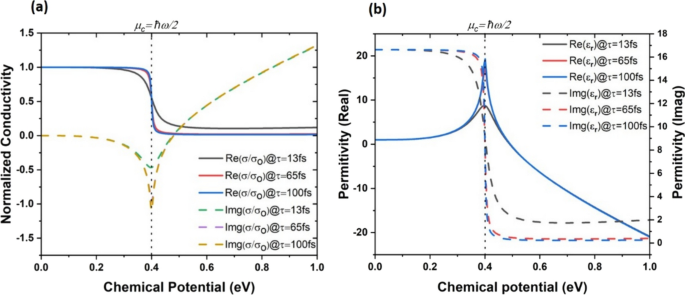
Graphene properties: a complex conductivity, b complex permittivity as a function of chemical potential simulated at λλ,
3 Results and analysis
3.1 Graphene-Si3N4 waveguide design and optimization
The effective mode index is a critical parameter in the design of the graphene EA optical modulator. The interaction between the optical mode distribution and the graphene layer plays an essential role in designing the graphene EA optical modulator. Optical absorption serves as a measure of this interaction, making it an essential factor to investigate when considering different waveguide configurations. The absorption can be calculated by:
Here is the constant for converting from m−1 to dB/µm, is the wavenumber and η is the imaginary part of the refractive index. Figure 3 shows the absorption for various dielectric layer thickness at τ=65 fs (mobility: 1466 cm2V−1 s−1) and explores how optical absorption varies with waveguide dimensions at the neutrality point (. It is observed that the transverse electric (TE) mode exhibits higher interaction with the graphene layer compared to the transverse magnetic (TM) mode. This discrepancy arises from the strong longitudinal electric field component present at the top interface of the Si3N4 waveguide, which contributes significantly to the interaction in the TE mode. However, the variation of has a very low impact in designing the optimum waveguide dimensions. Figure 3a illustrates the variation of absorption as a function of waveguide width , while maintaining a constant waveguide height of 300 nm. As the waveguide width increases, the absorption also rises, reaching its maximum value at a width of 1.2 µm. At this point, the largest absorption values for the TE and TM modes are 0.16 dB/µm and 0.023 dB/µm, respectively. Subsequently, the absorption remains almost constant as the waveguide width continues to increase. This behavior is attributed to the fact that the mode distribution is primarily concentrated in the waveguide and enlarges with the increment in the waveguide width up to 1.2 µm. In contrast, Fig. 3b demonstrates the absorption variation as a function of waveguide height, while maintaining a constant waveguide width of 1.2 µm. As the waveguide height increases, the absorption also rises, peaking at a waveguide thickness of 250 nm before gradually decreasing. This behavior arises from the interplay between the waveguide thickness and its interaction with graphene and the TE mode. At lower waveguide thicknesses, around 200–300 nm, the interaction with graphene and the TE mode is more pronounced, leading to the observed peak in absorption. This insight underscores the significance of optimizing the waveguide height for achieving optimal performance.
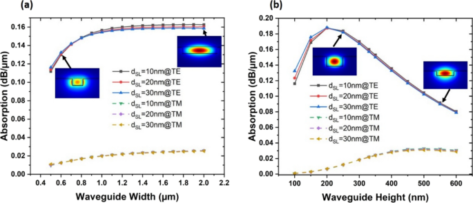
a TE and TM mode absorption as a function of waveguide width, b TE and TM mode absorption as function of waveguide height simulated at λλμμ,
3.2 Optimization of Si3N4 spacer for enhanced modulation efficiency
Following the optimization process, a TE Mode waveguide with a height of 300 nm and a width of 1.2 µm is chosen for subsequent simulations in order to achieve a single mode condition as well as maximum absorption. Figure 4a shows optical mode profile of the proposed modulator for a waveguide width and height 1.2 µm and 300 nm respectively at dielectric spacer thickness of 10 nm. The relationship between the TE effective refractive index and chemical potential, is investigated under various dielectric spacer thickness , and it shown in Fig. 4b at a scattering time of τ=65 fs. The real part of the refractive index, primarily responsible for phase changes, exhibits slight variations near the Pauli blocking threshold (μ) and then experiences a sudden shift as chemical potential increases from 0.5 eV to 1 eV. The changes in the real part of the refractive index within this region for of 10 nm, 20 nm, and 30 nm are 0.01, 0.008, and 0.007, respectively, indicating that a phase modulator can be effectively designed within this range (Sorianello et al. 2018, 2015). In contrast, the imaginary refractive index, mainly responsible for absorption, undergoes abrupt changes from μ due to the inter and intra band domination as explained in the previous section. The changes of imaginary refractive index for different dielectric thickness of 10 nm, 20 nm, and 30 nm are respectively which can be used to calculate the absorption using Eq. (4) and can be effectively designed an EA optical modulator in this region. Both the real and imaginary mode index increase with the reduction of dielectric spacer thickness which is due to the enhancement of the reciprocal action between the graphene and the optical modes. Based on these findings, we choose this specific range to design our EA optical modulator, which promises significant potential for achieving efficient and controllable modulation capabilities.
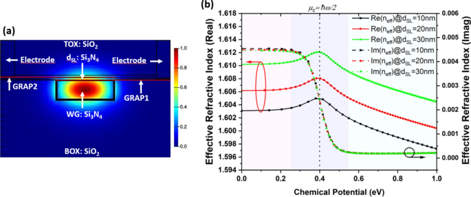
a Optical mode profile of proposed modulator (WWG = 1.2 µm and hWG = 300 nm), b Real refractive index (Re ηη) and Imaginary refractive index (Imag ηη) of fundamental TE mode as a function of under different at ττ
To explore the effects of chemical potential on graphene, a gate voltage is applied to the graphene capacitor, leading to a shift in its chemical potential. This alteration in the Fermi level subsequently influences the absorption properties of graphene. The investigation of the relationship between the gate voltage and the chemical potential of graphene is carried out using (Ye et al. 2014).
Here is the Fermi velocity, is the capacitance per unit length of the device and is the applied voltage where is the voltage corresponding to the charge-neutral Dirac point (=0.7 V). In Fig. 5a, the relationship between the gate voltage and the chemical potential is depicted for different of 10 nm, 20 nm, and 30 nm. The thicker dielectric spacers require higher voltages to drive the Fermi level of graphene compared to thinner dielectric layers . For instance, to reach the , the corresponding gate voltages required are 4 V, 6 V, and 10 V for of 10 nm, 20 nm, and 30 nm, respectively.
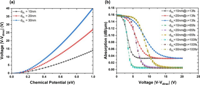
a Chemical potential at different voltages for of 10 nm, 20 and 30 nm at ττ, b TE mode absorption as function of applied voltage for of 10 nm, 20 and 30 nm at three distinct ττ
Based on the analysis above, we investigated of the optical absorption concerning the voltage applied to the graphene capacitor. Figure 5b illustrates the changes in absorption as a function of gate voltage for different , including 10 nm, 20 nm, and 30 nm. The curves are also plotted for three distinct values of τ (13 fs, 65 fs and 100 fs). While varying τ has a minor impact on the maximum absorption at lower voltages, it significantly affects absorption at higher voltages, leading to notable consequences for the modulator’s insertion loss (IL) and extinction ratio (ER). On the other hand, the voltage required to switch the graphene absorption from high to low strongly depends on . A thicker layer necessitates higher voltages for switching, thereby influencing the modulator’s efficiency and speed significantly. From Fig. 5b, we can now calculate essential parameters such as modulator’s efficiency, IL, and ER. Modulation efficiency is calculated by using:
here and represents the maximum and maximum absorption at corresponding minimum and maximum voltages and is the graphene length. In Fig. 6a, the modulation efficiency of devices with different graphene lengths is depicted for different (10 nm, 20 nm, and 30 nm) at three distinct values of τ (13 fs, 65 fs and 100 fs). It is shown that modulation efficiency is strongly influenced by factors of and τ. In particular, the efficiency increases with larger and decreases with decreasing . The quality of graphene also plays a substantial role in enhancing modulation efficiency; higher values of τ are associated with achieving greater modulation efficiency and vice versa. At a driving voltage of 12 V and a moderate τ (65 fs), the modulation efficiency for a 100 µm-long device is approximately 2.8 dB/V, 1.5 dB/V, and 1.10 dB/V for of 10 nm, 20 nm, and 30 nm, respectively. With the same driving voltage and device geometry, but with a smaller τ of 13 fs, the modulation efficiency is 2.2 dB/V, 1.2 dB/V, and 0.85 dB/V for of 10 nm, 20 nm, and 30 nm, respectively.
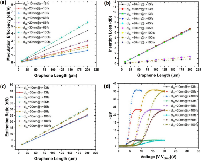
a Modulation efficiency, b insertion loss, c extinction ratio for different (10 nm, 20 nm and 30 nm) at three distinct ττ of the proposed modulator at 12 V driving voltage d) FoM for different (10 nm, 20 nm and 30 nm) at three distinct ττ at various voltages
The IL is determined at high forward voltage, where the absorption is quasi-minimal, while the ER is determined as the ratio of the maximum and minimum absorption at a driving voltage. Figure 6b and c presents the simulated IL and ER for the proposed modulators. IL is independent on but highly dependent on both τ and , whereas ER is almost independent of and τ but significantly influenced by . The extracted IL and ER for a driving voltage of 12 V and a device length of 100 µm are 0.65 dB and 15 dB, respectively, at of 30 nm with τ = 65 fs. In contrast, for τ = 13 fs, the IL and ER are 3.3 dB and 12.5, respectively, while keeping all other parameters, including the driving voltage and device geometry, constant. In summary, for the thinnest dielectric thickness, a longer graphene interaction length leads to higher modulation efficiency, while resulting in higher IL too. On the contrary, the better the graphene quality (higher τ), the higher the ER and lower the IL. Finding the right balance is crucial for optimizing the modulator’s performance.
In our investigation, we also analyze the figure of merit (FoM), a key metric frequently used for evaluating EA optical modulators which is defined by the ratio between the extinction ratio or modulation depth and insertion loss. Figure 6d illustrates the relationship between the FoM and the applied drive gate voltage for three distinct τ values (13 fs, 65 fs, and 100 fs), considering same (10 nm, 20 nm, and 30 nm). The FoM is significantly influenced by and τ. At a driving voltage of 12 V and a = 30 nm, the FoM shows rapid growth with improving graphene quality, reaching values as high as 12 at a higher scattering time (τ). Conversely, introducing lower-quality graphene with a shorter scattering time τ reduces the achievable FoM by a sixfold. On the contrary, has less significant control on the value of FoM directly but it can be revealed the operating voltage range of the devices to achieve a particular FoM. Our findings suggest that the thinnest layer with a higher τ provides the best optimum performance in terms of the modulator’s static characteristics. However, this evaluation does not provide information about the dynamic response of the devices and the optimum . Therefore, we also delve into the dynamic performance aspects, such as bandwidth and spectral range, which we discuss in the subsequent section.
3.3 Optimization of Si3N4 spacer for enhanced bandwidth
The frequency response of the device is determined using the electrical model depicted in Fig. 7a, which resembles the one employed in (Lee et al. 2021; Sorianello et al. 2015). In this model, represents a 50 Ω load resistance, is the sheet resistance of the graphene layers and is mainly influenced by the quality of the graphene transfer. signifies the contact resistance, which is dependent on the types of metal electrodes used. Within the graphene-insulator-graphene capacitance (), the oxide capacitance and the quantum capacitance of the two graphene layers are included. , being a series capacitance, reduces the total capacitance and enhances the speed. However, we have neglected this contribution in our simulations, as it is generally excluded in the characterization of graphene EA optical modulators. The electrical bandwidth can be calculated using the following equation.
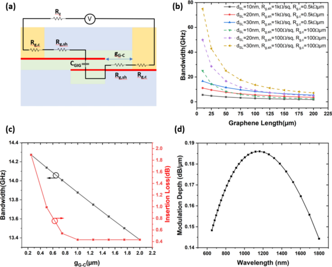
a Equivalent circuit model of the proposed modulator, b electrical bandwidth for different (10 nm, 20 nm and 30 nm) with two different and , c influence on bandwidth and insertion loss for 100 µm graphene length and 30 nm, d modulation depth dependence vs wavelength for broadband operation
Here is the total series resistance of the proposed modulator, represents the device capacitance and can be calculated using a straightforward parallel plate approximation, employing.
Here is the dielectric permittivity at the free space, is the dielectric permittivity is the Si3N4 assumed =6 (Giambra et al. 2019) is the waveguide, is length of the device and is the dielectric space between the graphene. The total resistance of the graphene modulator can be calculated by the following equation (Ji et al. 2019).
To estimate the electrical bandwidth of the proposed modulator, we assumed a graphene contact resistance of 500 Ω·µm and sheet resistance of 1000 Ω/sq (Canto et al. 2025; Lukosius et al. 2024). The distance between the metal and waveguide is considered . The estimated electrical bandwidth is depicted in Fig. 7b (solid line). The bandwidth is highly depending on the graphene length and it is decrease with increasing graphene length as the device capacitance also increases linearly. Moreover, the bandwidth is also prominently influenced by dielectric layer thickness, . Thicker layers lead to higher bandwidth due to the smaller capacitance. For example, at a graphene length of 100 µm, increasing the spacer layer thickness from 10 nm to 30 n, the bandwidth increases from 2.75 GHz to 8.5 GHz results in an approximately three-fold increase. By considering state-of-the-art contact resistance and sheet resistance of 100 Ω·µm and 100 Ω/sq (Abdollahi Shiramin and Van Thourhout 2017; Su et al. 2020). respectively, the bandwidth can be further increased to 13.62 GHz (shown in Fig. 7b with dotted line). Additionally, we also investigated the effect of metal electrode to waveguide distance on the bandwidth and insertion loss. Figure 7c shows the effect of the on the bandwidth and insertion loss IL for 100 µm graphene length and = 30 nm. The bandwidth is inversely related to the —it is higher for smaller and gradually decreases as the increases, primarily due to the linear rise in device sheet resistance. The bandwidth is inversely related to spacing and its high for a smaller spacing and linearly decreases with increasing the due to increasing the device sheet resistance linearly. On the other hand, insertion loss (IL) is higher at smaller and gradually decreases with increasing , stabilizing and remaining nearly constant beyond 1 µm. Therefore, finding the optimal trade-off between bandwidth and insertion loss is essential for designing an efficient modulator with both high speed and low loss. In our design, a 100 µm-long device with a 30 nm dielectric layer achieves a 13.62 GHz bandwidth and 0.46 dB insertion loss at a = 1.5 µm. Evaluating the modulator’s performance also encompasses its spectral characteristics. The investigation of these characteristics is displayed in Fig. 7d. Our proposed modulator boasts an operational bandwidth spanning from 650 to 1700 nm, accompanied by a modulation depth surpassing 0.16 dB/µm. As evident from Fig. 7d, our configuration encompasses a wide broadband operational spectral range, spanning 1050 nm. This extensive spectral coverage is attributed to the Si3N4 waveguide’s substantial energy gap, resulting in an ultra-wide light transparency window ranging from 400 to 2350 nm (Su et al. 2020; Wörhoff et al. 2015).
Table 1 provides a comparison between previously reported double layer graphene modulators and the proposed design, based on key performance metrics such as spacer layer material, modulation depth, modulation efficiency, insertion loss, and operating bandwidth. Notably, the proposed modulator demonstrates better performance in terms of modulation efficiency and operating bandwidth compared to prior work.
3.4 Conclusion
In summary, we have designed and analyzed Si3N4 based waveguide-coupled double-layer graphene EA optical modulators with Si3N4 as dielectric spacer layer between the graphene using the graphene surface conductivity model for various graphene length ranging 10–200 µm and for different dielectric spacer layer thickness (10 nm, 20 nm and 30 nm) between the graphene layer by considering various graphene quality. Notably, a 100 µm long device with a spacer of 30 nm demonstrates a high extinction ratio of 15 dB, insertion loss of 0.65 dB, and FoM of approximately 12 at an optical wavelength of 1550 nm by applying approximately 12 V. Additionally, the proposed design exhibits a high bandwidth of 14 GHz. These findings underscore the potential of the modulator for high-speed optical on-chip communication applications.