Article Content
1 Introduction
Silicon carbide (SiC) is a third-generation semiconductor material that offers significant advantages over traditional silicon (Si), particularly for high-power, high-frequency, and high-temperature applications. SiC surpasses Si in several key areas, such as a wider bandgap, higher thermal conductivity, and a superior breakdown electric field [1–2]. These properties make it an ideal candidate for power electronics, electric vehicles, and renewable energy systems. Furthermore, silicon carbide (SiC) can be utilized as a sensor for analyzing plasma dynamics generated by the interaction between lasers and various gases [3]. SiC detectors demonstrate a linear response to fluctuations in plasma intensity, facilitating accurate temporal characterization and analysis of plasma evolution. However, SiC also presents challenges [4–5]. Therein, to construct high-quality, polymorph-stable, and large-diameter SiC substrate wafers while reducing defect density, substrate warping, and residual stress are the primary issues and challenges outlined in Literature 4. In contrast, Literature 5 focuses on the types and characteristics of defects and impurities in SiC, as well as doping technologies. It further investigates the challenges in controlling these impurities and defects to optimize the material’s performance in semiconductor applications. The cost of SiC materials is substantially higher than that of Si due to the complexities involved in producing high-quality SiC wafers and the specialized fabrication techniques required. Additionally, SiC’s greater hardness and brittleness necessitate advanced processing methods, leading to increased manufacturing costs and reduced yield compared to Si. Despite these drawbacks, the potential for SiC in next-generation electronic devices continue to drive research and investment in overcoming these challenges.
After silicon carbide (SiC) is sliced into wafers from the crystal ingot through wire cutting, it undergoes grinding and chemical mechanical polishing (CMP) to achieve a surface with low roughness [6], thereby enhancing the quality of subsequent processing steps. However, during the CMP process of SiC, a significant amount of time and consumables, such as polishing heads, are required, leading to an increase in wafer manufacturing costs. As a result, some studies have explored the incorporation of various materials into the polishing slurry to enhance the material removal rate (MRR) of SiC and reduce its surface roughness [7]. Nevertheless, this method remains a wet process, requiring substantial consumables and additional wafer cleaning steps. Hsieh et al. [8] discussed the SiC wafering steps and the corresponding purposes and compare the three configurations of SiC CMP currently employed in the industry. They also reviewed the oxidation behaviors and polishing performance of hybrid CMP technologies, such as electro-CMP (ECMP), photocatalytic CMP (PCMP), gas-PCMP, and ultrasonic-ECMP.
Laser systems are versatile tools that can be used for marking, cutting, drilling, ablation, and surface modification of materials. Torrisi et al. [9] explored the correlation between laser wavelength and the ablation threshold of materials. Their study revealed that lasers with shorter wavelengths, such as ultraviolet light, exhibit higher photon energy, enabling stronger interactions at the material surface and more effectively breaking chemical bonds within the material. As a result, these lasers demonstrate lower ablation thresholds. In contrast, as the wavelength increases, the laser’s penetration depth into the material grows, energy absorption efficiency decreases, and the lower photon energy primarily manifests as heat, leading to a higher ablation threshold. (Reviewer#9; Question#3) In addition, femtosecond [10–11], picosecond [12], hybrid-CO2 [13], and nanosecond [14] laser systems have been applied to modify the surface characteristics of silicon carbide (SiC) in prior research. Femtosecond lasers offer exceptional precision in material removal, particularly beneficial for polishing SiC due to their ultra-short pulse durations. This results in minimal thermal effects, reducing the risk of cracks and ensuring a smaller heat-affected zone (HAZ). The process leads to fewer defects and smoother surfaces, optimizing conditions for subsequent chemical mechanical polishing (CMP) process. However, the femtosecond laser systems come with high costs and require intricate parameter control, and their material removal rate is lower, resulting in longer processing times. On the other hand, nanosecond lasers, with their longer pulse durations, can achieve higher material removal rates, significantly enhancing processing efficiency. These lasers are more accessible for industrial use due to their lower cost and simpler operation. Nevertheless, nanosecond lasers create a larger HAZ, increased oxidation, and higher surface roughness, which are drawbacks in precision applications. Thus, femtosecond lasers are preferable for applications requiring precision and surface quality, whereas nanosecond lasers are suitable for scenarios prioritizing processing speed and cost-effectiveness.
Studies such as that of Zhang et al. [15] have explored the effects of laser parameters on surface roughness, ablation depth, and oxidation of SiC. In this study, the pulsed femtosecond laser with wavelength of 1064 nm and pulse duration of 10–15 fs was employed. Their findings indicated that the laser ablation threshold for SiC ceramics is approximately 0.355 J/cm². Notably, as pulse energy increased, surface roughness initially decreased before rising again. Additionally, increasing the laser’s defocus amount led to a reduction in polishing depth and an increase in surface roughness. These results are critical for optimizing laser processing techniques for SiC ceramics. Lin et al. [16] explored the influence of varying spot overlap ratios by the femtosecond laser planarization process on SiC ceramics. In their experiments, they kept the single pulse energy and laser incident angle while adjusting the laser repetition frequencies and scanning speeds to achieve different spot overlap ratios. Their findings demonstrated that both ablation depth and surface roughness remained relatively consistent at stable spot overlap ratios, irrespective of changes in repetition frequency or scanning speed. Additionally, surface oxidation decreased significantly when the spot overlap ratio fell below 90%, suggesting that variations in overlap ratios could serve as a valuable guideline for selecting optimal processing parameters. Xie et al. [17] utilized a femtosecond laser to irradiate a SiC substrate to enhance the efficiency of subsequent chemical mechanical polishing (CMP) process. By adjusting parameters such as laser fluence, focus position, scanning speed, and scanning interval, they discovered that Si-O compounds formed on the laser-irradiated SiC surfaces. This resulted in a reduced hardness, which is beneficial for the CMP process. Furthermore, lower surface roughness and fewer defects were achieved when the process was conducted in an oxygen atmosphere, as oxygen actively participated in the photochemical reactions. Chen et al. [18] employed femtosecond laser irradiation to accelerate the chemical mechanical polishing (CMP) process of SiC. The experimental results revealed that the ablation threshold of the carbon (C) face of SiC is lower compared to the silicon (Si) face. Furthermore, under the same laser fluence, the hardness of the C face of the laser irradiated SiC sample was higher than that of the Si face. Post-laser irradiation, the material removal rates during CMP were significantly improved, with the C face and Si face demonstrating enhancements of 77% and 207%, respectively. Zhang et al. [19] conducted a study using a high repetition frequency femtosecond laser at a wavelength of 1030 nm to modify the surface of SiC ceramics. They explored the impact of various parameters on surface quality, material removal rate, and surface oxidation. The experimental results demonstrated that increasing the laser scanning pitch can significantly reduce surface oxidation. Additionally, the optimal material removal rate was achieved with a laser fluence of 0.4 J/cm² at a pulse width of 470 femtoseconds.
Duc et al. [20] presented the infrared (1064 nm) nanosecond pulse laser ablation on SiC and analyze its ablation depth and surface morphology under various fluence values. Both it and this study use nanosecond laser sources and explore the influence of laser fluence and ablation depth. The results showed that the ablation threshold was determined by the absorption coefficient of SiC at infrared wavelength, and the absorption coefficient dependence on the doping concentration and temperature. The change of temperature also affected the ablation behavior and dimension such as the diameter and depth. Chen et al. [21] employed a nanosecond laser to induce different cluster sizes and oxide content on the Si-face of a SiC substrate. The experimental results revealed that as the oxygen content and oxide composition uniformity on the surface increased, the stability of the material removal rate (MRR) in chemical mechanical polishing (CMP) was enhanced, thereby improving removal efficiency. This suggests that controlled laser-induced oxidation can optimize the CMP process for SiC substrates, leading to better performance in precision machining. This research mainly prepares oxides with loose structure, content greater than 50 wt%, and uniform composition to accelerate grinding. Wang et al. [22] presented a new method by using the nanosecond laser irradiation as the pre-process for CMP process of single crystal 4 H-SiC. In addition, the performance such as the material removal rate (MMR) and surface roughness of nanosecond laser irradiation assisted CMP (NLIA-CMP) were discussed. The results showed that the MMR can be significant improved by the NLIA-CMP with low surface roughness. Specially, the MMR of NLIA-CMP was 9.22 μm/h under the laser parameters of low scanning interval, low scanning rate, and long pulse width. This article is mainly about finding the laser irradiation parameters that can provide the best MMR to assist the CMP process. An et al. [23] used the nanosecond laser to irradiate the reaction-bonded SiC (RB-SiC) and analyzed its change in surface characteristics. The results indicated that the hardness of RB-SiC can be reduced by up to 40.7% by laser irradiation, and the softening degree of RB-SiC was strongly related to laser parameters. This method can provide an improvement for removability of RB-SiC composite material. This article constructs the relationship between softening degree and laser irradiation conditions. In addition to exploring the effects and causes of laser ablation depth and hardness of materials, the article proposed in this study also hopes to directly ablate and grind SiC by adjusting laser parameters in the future. Zhang et al. [24] explored that changes in the mixing ratio of plasticizers, additives, and cross-linking agents have a significant impact on the mechanical properties of starch-based foam materials. Among them, through optimizing the formula, starch/ethylene vinyl acetate (EVA) foam materials were developed in the research, which improved the mechanical strength. In the analysis, a simple and accurate prediction of tensile strength and resilience was made based on the mixing ratio of starch-based/EVA foam material composition. This research mainly increases and predicts the mechanical strength through the optimization of the material’s formula. The presented research uses laser surface modification technology to reduce its mechanical strength. Both technologies optimize the material properties for specific needs, which are complementary technologies.
UV lasers, due to their shorter wavelength and higher photon energy, can efficiently break molecular bonds and vaporize SiC material with high precision and minimal thermal effects. Compared to UV lasers, green lasers have lower absorption efficiency in SiC, making them less effective for fine and precise ablation, although they may be suitable for removing thicker layers. Infrared lasers, while capable of deeper penetration and higher power ablation, typically result in less controlled ablation and greater thermal damage due to their lower absorption efficiency in SiC. Thus, UV lasers are the optimal choice for SiC ablation, particularly for applications requiring precision and minimal thermal impact. This study proposes the use of ultraviolet (UV) ablation, stable material removal on SiC surfaces, and simultaneously removes the defects remaining from previous machining such as wire cutting. The laser, with a pulse width of 30 nanoseconds, offers advantages such as lower maintenance costs compared to femtosecond lasers, higher operational stability, and suitability for prolonged operation. Its longer pulse duration enables higher energy density per pulse, facilitating an enhanced material removal rate, particularly for high-hardness materials like SiC. The controlling parameters of laser system include different scanning speeds, overlap rate, and repetition counts. After material removal, the removal depth of SiC under various parameters is analyzed using the three-dimensional confocal laser scanning microscopy, while nano-indentation tester is employed to assess the hardness of SiC. Additionally, the energy dispersive X-ray spectroscopy (EDS) and X-ray diffractometer (XRD) are used to analyze the effects on the material composition and crystal lattice structure, respectively. Finally, the SiC wafers after dry material removal were wet polished, and the consumption of the polishing head and the wet grinding removal thickness under the same grinding amount and different laser dry removal repetition times were analyzed. The results proposed in this study will be able to provide important reference parameters for laser material thinning of SiC in the future and reduce the process and cost of wet grinding in industrial applications.
2 Experimental procedure
2.1 Experimental system
The laser assisted polishing system comprised a solid-state Q-switched ultraviolet laser with wavelength of 355 nm (Coherent, Inc., AVIA NX 355 − 20), which was used for ablation of SiC substrate after wire cutting. The maximum power of the laser system is 20 watts (W), and all dry ablation experiments on SiC were conducted using this power level in this study. In the experimental process, the laser repetition frequency was fixed at 100 kHz, corresponding to a single pulse energy of 200 µJ. The pulse duration was 30 ns at repetition frequency of 100 kHz. The scanning speed was fixed at 1000 mm/s, with the number of repetitions ranging from 1 to 50. The complete laser specifications and experimental parameters is summarized in Table 1. A dual-axis galvanometer scanning system was employed for two-dimensional scanning of the processing area. The focal length of the telecentric focusing lens is 580.8 mm, and the laser spot size at a single point is approximately 45 μm. Calculated from the above pulse energy and laser spot size, the laser fluence used in this study was approximately 12.6 J/cm2. Through preliminary testing, it was found that the threshold fluence of SiC ablation needs to be greater than 6.3 J/cm2 to have a significant material removal effect on SiC. The schematic of the laser ablation system used on the SiC substrate is shown in Fig. 1.
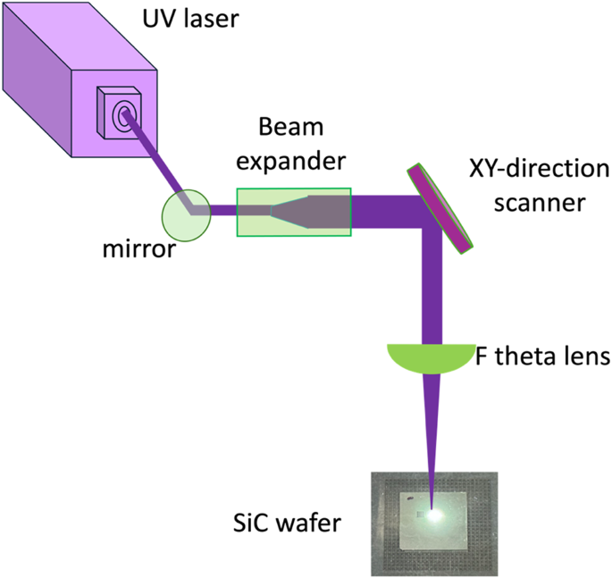
Schematic of laser dry ablation on SiC wafer
For subsequent analysis of ablation depth, surface roughness, and hardness, each laser dry ablation area was set to 1 × 1 mm. Additionally, since a larger area is required for X-ray diffraction (XRD) to accurately measure the lattice structure, the sample area for each set of parameters was designated as 20 × 20 mm.
During the two-dimensional surface scanning ablation of the SiC substrate, the spacing between laser spots significantly affects the ablation depth and surface roughness of the substrate. The spacing of two laser spots in the x-direction (Δx) is influenced by the scanning speed, while the y-direction spacing (Δy) of two laser spots is affected by the overlap rate. The overlap rate (OR) in the y-direction can be calculated based on the bite size (Bs) between laser spots and the spot diameter (D), as expressed in Eq. (1). The spacing between laser spots in x and y directions was shown in Fig. 2.
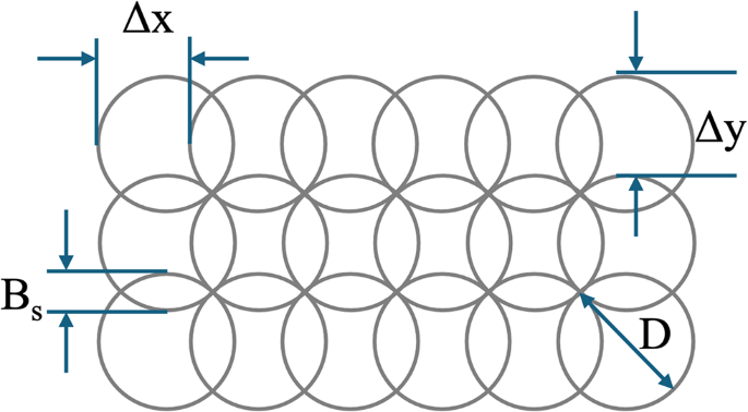
Schematic of the spacing of laser spot in x and y directions
2.2 Surface characteristics measurement
In this study, several advanced characterization techniques were employed to analyze silicon carbide (SiC) materials subjected to laser dry ablation. First, a three-dimensional confocal laser scanning microscopy (KEYENCE, VK-X200) and its analysis software were utilized to assess the removal depth and surface roughness of the SiC samples post-ablation. This technique provides high-resolution, three-dimensional imaging, enabling precise measurements of surface features and variations in topography. Its non-contact nature allows for the analysis of delicate surfaces without inducing additional damage, making it particularly suitable for evaluating the effects of laser processing on material integrity. Second, the scanning electron microscopy (SEM) coupled with energy dispersive X-ray spectroscopy (EDS) was employed for compositional analysis of the SiC materials. SEM can offer high-resolution imaging of the sample surface. The EDS detector measures the energy and intensity of the elements emitted X-rays, allowing for the identification and quantification of the elemental constituents of the SiC, thereby facilitating an understanding of any compositional changes resulting from the laser ablation process. Third, X-ray diffraction (XRD) was employed to investigate the crystalline structure of the SiC samples. XRD is a powerful analytical tool that provides information about the crystal phases, lattice parameters, and crystallinity of the material. By analyzing the diffraction patterns, one can discern changes in the lattice structure that may occur as a result of laser processing, offering valuable insights into the material’s structural integrity. In the measuring process, the scan type was theta-2theta scan (θ-2θ Scan), and the 2theta ranges from 20 to 80 degrees with increasement of 0.08 degrees. Finally, the nano-indentation tester (Anton Paar, NHT3) was conducted to evaluate the hardness of SiC before and after laser dry ablation. This technique utilizes a sharp indenter to penetrate the material’s surface under controlled loading conditions, providing accurate measurements of hardness at the nanoscale. The results offer characteristics into the mechanical properties of SiC following the ablation treatment. The above characterization techniques provide a comprehensive evaluation of the effects of laser dry ablation on SiC materials, elucidating the interplay between surface morphology, compositional integrity, mechanical properties, and crystallographic structure.
3 Experimental results and discussion
3.1 Surface characteristics under various overlap rate
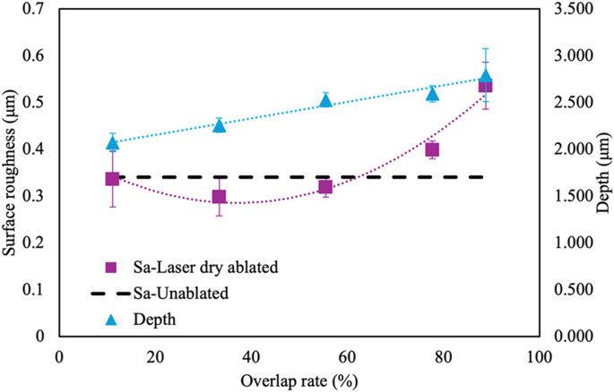
At the initial stage of the experiment, different scanning speeds were employed to observe the overlap effects of the laser spot in the x-direction. To ensure the laser energy is fully applied to the SiC substrate, partial overlap of the laser spot in the x-direction was desired to prevent regions of the material from remaining unaffected by laser ablation. As illustrated in Fig. 3, when the scanning speed was set to 1250 mm/s, certain areas of the material were not ablated by the laser. However, when the speed was reduced to 1000 mm/s or lower, the laser spot exhibited overlap in the x-direction. To enhance the surface treatment efficiency, the scanning speed was fixed at 1000 mm/s in this study. Subsequently, the effects of varying the overlap rate (OR) in the y-direction on laser dry ablation were analyzed in terms of depth, surface roughness, ingredient weight, and hardness. Prior to laser dry ablation, the surface roughness was approximately 0.34 μm. Through the laser dry ablation with different overlap rates, the surface roughness initially decreased with increasing OR, reaching its lowest value of less than 0.3 μm at an OR of 33.3%. However, when OR exceeded 60%, the significant overlap of laser spots and repeated ablation of SiC resulted in a substantial increase in surface roughness, reaching 0.54 μm at an OR of 88%, as shown in Fig. 4. The relationship between roughness and OR can be fitted with a second-order polynomial equation, and its correlation R2 is 0.96. On the other hand, the ablation depth increased with higher overlap rates, ranging from 2.1 μm to 2.8 μm. This relationship between depth and OR can be fitted by a linear equation, and its correlation R2 is 0.97. The possible reason for this phenomenon is that when the overlap rate is low, the laser can selectively remove surface irregularities, mainly by ablating uneven areas and reducing protrusions to smooth the surface. This results in a reduction in surface roughness without significant thermal damage or microstructural alteration, preserving the surface’s integrity. However, when the overlap ratio exceeds 60%, the increased overlap intensifies localized heat accumulation. This leads to excessive material melting and subsequent non-uniform re-solidification, forming irregular surface textures. Additionally, repeated laser exposure may induce microcracks, voids, or the redeposition of ablated material, all of which contribute to a rougher surface. This combination of thermal effects and material redistribution results in increased surface roughness with higher overlap ratios.
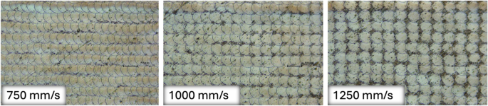
The optical image of SiC treated by UV laser with varying scanning speed along the X direction
Surface roughness and depth of SiC following laser dry ablation with varying overlap rates
Moreover, microscopic imaging results reveal that at lower OR values (OR = 11.1–55.5%), the accumulated laser energy density remains relatively low, resulting in minimal color change on the ablated SiC surface, which closely resembles the original SiC color. However, as the OR increases (OR = 77.7% or even 88.8%), the accumulated energy density rises correspondingly, leading to a gradual darkening of the SiC surface, as shown in Fig. 5. This surface darkening can adversely affect the accuracy of thickness detection during subsequent fine polishing. Therefore, in laser ablation studies, it is crucial to maximize the ablation depth while minimizing surface color changes.
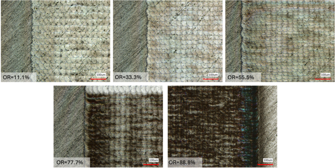
The optical image of SiC treated by UV laser with varying overlap rates along the Y direction.
SEM observations at 5k magnification reveal distinct changes in the surface morphology of SiC under varying overlap ratios (OR), as shown in Fig. 6. For OR values below 60%, the surface remains relatively uniform and smooth, characterized by faint outlines corresponding to the laser spot peripheries. No significant material reorganization is observed, indicating minimal thermal effects. However, when the OR increases to 77.7% or higher, noticeable morphological changes occur due to intensified thermal effects. These include material redeposition manifesting as ridges or particulate formations. These features are indicative of localized melting and re-solidification processes, which disrupt the surface uniformity and increase roughness.
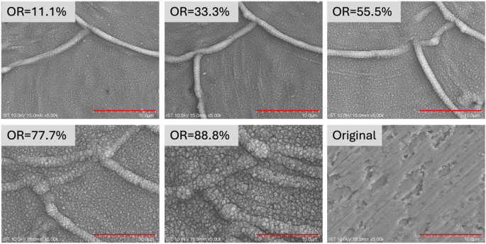
The SEM image of SiC treated by UV laser with varying overlap rates along the Y direction.
To investigate whether the color change after laser dry ablation is related to the composition and oxidation level of SiC, the samples were subjected to EDS analysis using SEM. The measurement results revealed that, prior to laser dry ablation, the ingredient weight% of C, O, and Si were 30.2%, 1.26%, and 68.54%, respectively (as shown in Fig. 7). However, after laser dry ablation, the proportions of C and Si decreased with increasing OR. Notably, even after a very low overlap rate (OR = 11.1%), the proportion of C sharply declined, converting into O atoms due to oxidation. At a high overlap rate (OR = 88.8%), the C content dropped to just 6.2%, while the O content increased to 40.4%. This indicates that the surface of SiC undergoes significant oxidation following laser dry ablation, which is beneficial for subsequent wet polishing processes.
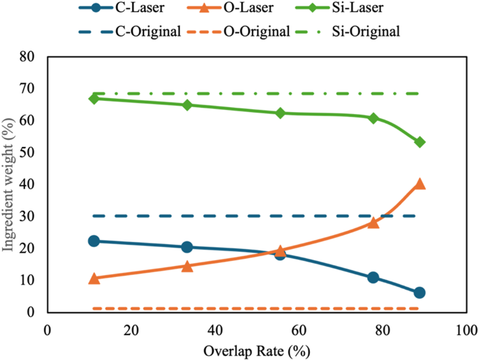
Ingredient weight of SiC after laser dry ablation with varying overlap rates
Additionally, we used XRD to measure the lattice structure changes of SiC after laser dry ablation. In the Fig. 8, the x-axis corresponds to the diffraction angle (2θ) in degrees, while the y-axis denotes the intensity of the diffracted X-rays, providing insights into the crystalline structure of the material. Therein, theta-two theta mode will have different penetration depths depending on the incident angle. In this experiment, the incident angle range is 20–80 degrees, and the penetration depth falls between 13 and 50 μm. Therein, the penetration depth at 60 degree was 39 μm. Before laser dry ablation, the lattice structure was hexagonal Silicon Carbide. However, after undergoing laser dry ablation (with OR between 11.1% and 55.5%), the original lattice was disrupted, resulting in the formation of cubic Silicon and hexagonal Moissanite-5 H Silicon Carbide structures, shown as Fig. 8. When the overlap rate increased beyond 77.7%, leading to excessively high laser energy density, the lattice structure of hexagonal graphite carbon could also be detected. These results indicated that the laser process may have caused the dissociation of SiC and the formation of free carbon on the surface. These findings demonstrate that significant changes in the lattice structure of SiC occur after laser dry ablation, which may further affect its hardness.
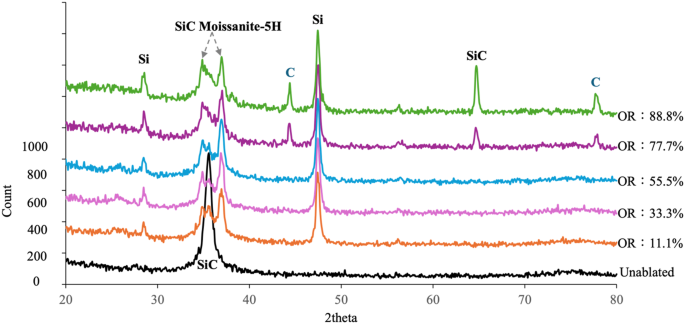
XRD diagram of SiC before and after laser dry ablation with varying overlap rates
Using a nano-indentation tester to measure the hardness before and after laser dry ablation, the experimental results revealed that the original hardness of SiC was approximately 11.3 GPa. However, after laser dry ablation, although the overlap rate OR was only set to 11.1%, its hardness significantly dropped to 0.28 GPa, which is only 2.52% of the original hardness. The hardness further decreased as the overlap rate increased, reaching just 0.03 GPa at an OR of 88.8%, representing a hardness ratio of 0.27%, shown as Fig. 9. These results indicate that due to changes in the lattice structure and ingredient weight of SiC, the hardness of SiC dramatically declines after laser dry ablation. Compared with An et al. [23] who used nanosecond laser to irradiate silicon carbide (RB-SiC) and reduced the hardness by 40.7%, the hardness of this experimental result is only less than 3% of the initial value. Subsequent material removal of CMP process can provide greater benefits than the SiC without laser ablation. To maintain the original wafer color and achieve higher processing efficiency during laser dry ablation, an optimal overlap rate of 55.5% was selected. Under this condition, the surface roughness can also be maintained at levels similar to those before laser dry ablation.
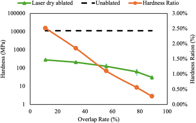
Hardness of SiC before and after laser dry ablation and its hardness ratio at different overlap rates
3.2 Surface characteristics under various repetitions
Since the depth of a single laser dry ablation pass is only about 2 μm, industrial applications aim to remove 20–30 μm from a single side of a SiC wafer via laser dry ablation to eliminate the coarse grinding step in chemical mechanical polishing. To achieve this, the ablation depth can be increased by raising the number of laser repetitions. In the experiment, the number of repetitions for a single area was set to 1, 5, 10, and 50 times, with the surface roughness and ablation depth analyzed for each case. The experimental results revealed a highly linear relationship between the ablation depth and the number of repetitions, with the depth reaching approximately 26 μm after 50 repetitions. Surface roughness increased rapidly with the number of repetitions from 1 to 10, but after exceeding 10 repetitions, the rate of change in surface roughness slowed down (as shown in Fig. 10).
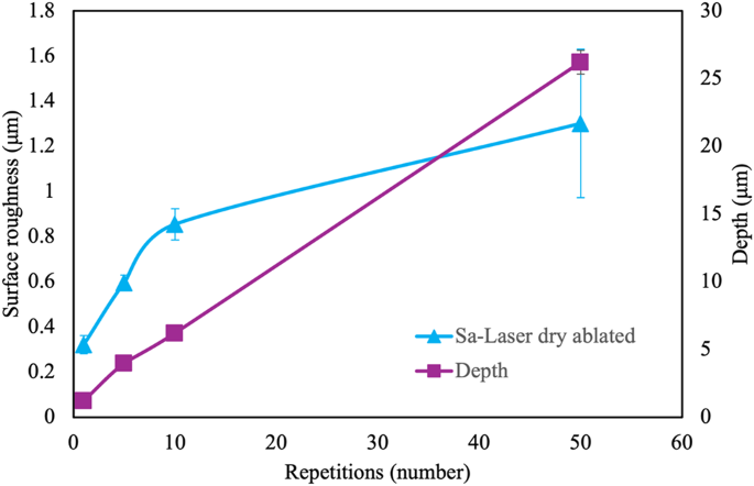
Surface roughness and depth of SiC after laser dry ablation with an overlap rate of 55.5% and varying repetitions
Furthermore, the linear relationship between the number of repetitions and the ablation depth of SiC reflects consistent energy deposition and ablation mechanisms with each laser pass, enabling gradual and uniform material removal. In contrast, the correlation between ablation depth and overlap rate (OR) is less pronounced (Fig. 4). This distinction arises because increasing the OR effectively acts as additional exposure, but unlike discrete repetitions, a higher OR concentrates laser thermal energy into a smaller area due to overlapping pulses. This overlap results in localized heat accumulation, leading to phenomena such as excessive melting and material redeposition. These effects may limit the efficiency of material removal and restrict the achievable ablation depth.
The divergence between repetitions and overlap rate lies in the spatial and temporal distribution of laser energy. Multiple passes (repetitions) allow the surface to cool between exposures, maintaining a consistent ablation rate. Conversely, a high OR compresses energy application spatially, generating localized thermal gradients and altering ablation efficiency. These findings underscore the importance of carefully balancing repetitions and overlap rate to optimize ablation depth while preserving surface quality.
Additionally, the hardness initially decreases with the increasing number of repetitions. However, after more than five repetitions, the variation in hardness becomes minimal, stabilizing in the range of 55–75 MPa (shown as Fig. 11). This indicates that the hardness of SiC can be significantly reduced after just one or a few scans, and further increasing the number of repetitions mainly benefits the ablation depth with little additional effect on the hardness.
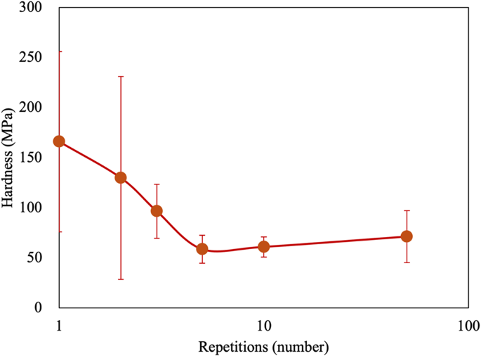
Hardness of SiC after laser dry ablation with an overlap rate of 55.5% and varying repetitions
The reduction in the hardness of silicon carbide (SiC) after laser processing is primarily a result of the combined thermal and structural effects caused by high-energy laser interactions with the material. Key contributing factors are: (1) Thermal effects leading to phase transformations: The intense localized heat generated during laser processing induce phase transformations in the SiC crystal structure. (2) Surface oxidation: The high temperatures facilitate the oxidation of the SiC surface, forming a softer silicon oxide layer or increasing oxygen content. This oxidation layer lacks the mechanical strength of SiC, resulting in reduced hardness. (3) Material removal and residual stress: The rapid heating and cooling cycles inherent to laser processing introduce thermal gradients that may lead to microcracks or residual stress within the material. These effects compromise the structural cohesion, further lowering hardness.
On the other hand, the hardness of SiC decreases as the number of laser scans increases from 1 to 5. This phenomenon arises because each successive scan removes a portion of the surface material, thereby reducing the crystalline structural integrity and altering the microstructure through localized heating, phase transitions, or the formation of microcracks. These changes cumulatively lead to a progressive reduction in material hardness. In the initial stages of scanning, the transformation of the SiC surface from its original state to a modified state may result in inconsistent ablation depths, irregular phase transitions or stress distributions. Additionally, changes in the properties of ablation by-products could further influence hardness measurements, leading to greater variability in the early scans. Furthermore, small-scale hardness testing methods, such as nano-indentation tester, are highly sensitive to local surface conditions, including roughness, residual stress, and subsurface defects. As a result, measurement errors are magnified during the early stages of ablation. After five scans, the hardness stabilizes and remains nearly constant. This stabilization is likely due to the majority of the high-hardness surface layer being either ablated or modified, leaving behind a more uniform altered layer with consistent properties. Furthermore, repeated scans may bring the surface material to a thermal equilibrium state, where additional heating or energy deposition no longer induces significant changes.
3.3 Wet griding effect after laser dry ablation
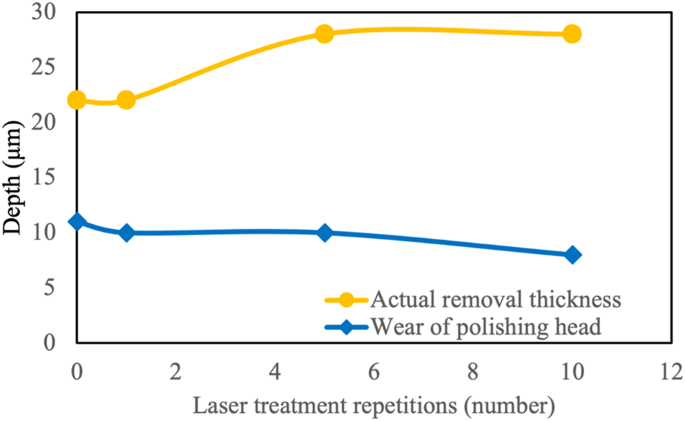
After completing the preliminary analysis of laser parameters on small areas of SiC surface, the entire 4-inch SiC wafer was subjected to laser dry ablation using a power of 20 W, a pulse repetition frequency of 100 kHz, a scanning speed of 1000 mm/s, and an overlap rate of 55.5%. Each full scan of 4-inch SiC wafer took approximately 10 min, and the wafer was scanned with repetitions of 1, 5, and 10 times, respectively. Subsequently, a wet CMP process was carried out and compared with SiC that had not undergone laser dry ablation. During the wet CMP process, the removal target was set to 30 μm for all wafers. After grinding, the actual material removal and the consumption of the polishing head were measured.
The experimental results revealed that for the wafers with no laser dry ablation and after just one scan, the actual wet grinding removal was 22 μm, which only achieved 73% of the target removal rate. However, for wafers scanned five and ten times, the wet grinding removal reached 28 μm, achieving 93% of the target removal rate, shown in Fig. 12. Furthermore, the consumption of the polishing head decreased slightly as the number of laser dry ablations increased. The polishing head’s wear for wafers with no laser dry ablation was approximately 11 μm, whereas after five and ten laser ablation passes, the wear reduced to 10 μm and 8 μm, respectively. These results confirm that laser dry ablation facilitates the rapid removal and thinning of the SiC surface material, thus benefiting subsequent wet chemical mechanical polishing by increasing the target removal rate and reducing the wear of the polishing head.
Grinding depth and head consumption during CMP process after varying repetitions of laser treatment on SiC
Among them, although the significant reduction in SiC hardness after laser treatment, the material removal thickness during grinding with a single repetition of laser processing remains nearly identical to that of untreated SiC. This may be attributed to the formation of a thin, dense residual layer or alterations in the surface microstructure during the laser ablation process, which resist initial grinding and require similar force or time for removal as untreated SiC. Another key reason is that the laser ablation depth (only 1.2 μm under one repetition) is insufficient relative to the grinding penetration depth, resulting in minimal influence from the laser-treated layer and causing the grinding process to interact predominantly with the unaffected bulk material.
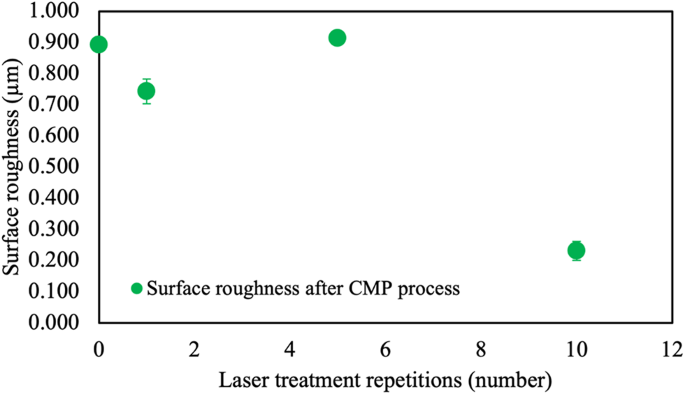
After laser thinning and CMP polishing, the surface characteristics of the SiC wafer such as surface roughness are also analyzed. From the measurement results, it was found that the surface roughness of the SiC wafer without laser treatment and after laser treatment once and five times, and after CMP process, was approximately 0.7–0.9 μm. After 10 times of laser treatment and CMP process, the surface roughness dropped to 0.23 μm, shown in Fig. 13. The reason may be that increasing the number of laser treatments can ablate more material from SiC and may remove internal defects. After CMP process, it can have better surface roughness than when the number of laser treatments is less.
Surface roughness during after varying repetitions of laser treatment on SiC and CMP process
4 Conclusion
This study provides compelling evidence that laser dry ablation can significantly enhance the surface processing of SiC wafers, presenting a highly efficient alternative to conventional chemical mechanical polishing (CMP). By employing optimized laser parameters, including a power of 20 W, scan speed of 1000 mm/s, and an overlap rate of 55.5%, we achieved considerable material removal rates, with improvements in both surface roughness and hardness reduction. Notably, after just one pass of laser dry ablation, the hardness of SiC can be reduced to less than 3% of its original value. Furthermore, the material removal depth can be significantly increased by raising the number of laser ablation passes. After 50 repetitions of laser scanning, the removal depth reaches nearly 30 μm. This highlights the efficiency of laser dry ablation in both reducing material hardness and achieving considerable material removal, making it a promising technique for applications requiring precise and deep surface modifications. Additionally, SiC wafers that underwent five and ten laser ablation passes showed a remarkable material removal efficiency of 93% during subsequent wet grinding, compared to only 73% for untreated wafers. Moreover, the wear on polishing heads decreased by approximately 27%, offering substantial cost savings in consumable materials. These results demonstrate that laser dry ablation is not only effective in removing surface material but also in minimizing wear on tools, making it highly advantageous for industrial-scale applications. This innovative approach could streamline SiC wafer thinning processes, shorten production times, and enhance the overall efficiency of semiconductor manufacturing. At present, the potential limitation of this work is to produce a surface with extremely low surface roughness. In the future, the surface roughness will be further optimized through parameter adjustment, hoping that the surface roughness will be less than 30 nm. In the future, the residual damage induced by laser ablation on SiC materials, including subsurface microcracks, heat affected zone, thermal damage, or amorphization, will be extensively investigated. Such damage may alter surface morphology, degrade material properties, or introduce stress fields, thereby affecting the uniformity and quality of SiC layer removal during subsequent CMP processes. Ultimately, these effects could compromise the precision and performance of semiconductor device fabrication.