Article Content
Introduction
Free charge carriers such as electrons are essential components of our modern-day world. They facilitate devices such as smartphones and computers. Uncontrolled or undesired charges, on the other hand, can cause damage and reduce the performance of such devices. Prominent examples are gate-oxide breakdown in flash memory1 and charge-noise on the nanoscopic level2,3. The detection and quantification of desired and undesired charge carriers with electrometers4,5 holds significant technological importance on the nanoscale.
Despite significant progress5,6,7,8,9,10,11,12,13,14,15,16, electrometers have to date been unable to provide time-resolved access to elementary charges with subnanometer resolution. Precisely resolving charges and performing temporal analysis at atomic lattice scales, however, is becoming increasingly important. For example, the investigation of 2D ferroelectric systems would greatly benefit from the use of a highly sensitive electrometer, which could provide critical insights into the unresolved foundational aspects of their physical characteristics17. Furthermore, as silicon transistors reduce to sizes of a few nanometers they become more susceptible to charge-induced noise18,19.
Particularly, quantum technology applications face challenges: in ion-based quantum computers, localized electronic states are suspected to cause decoherence due to motional heating20; superconducting qubits suffer from defect-induced charge-noise21,22; in atom-like spin qubits in wide-bandgap semiconductors, charge-noise leads to optical and spin decoherence5,13,23,24,25, significantly limiting the development of quantum networking and sensing26,27.
Understanding the underlying mechanisms of such platform-specific detrimental processes is a necessity to improve the performance and application range of nanoscale electronic and photonic devices including open questions around decoherence processes, electron dynamics, and material questions of lattice defect formation.
Here, we introduce a quantum electrometer that enables the detection of electric fields produced by single and multiple elementary charges with a relative sensitivity of 10−7 and resolves individual charge state dynamics down to tens of nanoseconds at the Ångström-scale.
The electrometer consists of an electric field-sensitive, optically active, local probe and a read-out unit (Fig. 1a). In this demonstration, the local probe is a negatively charged tin-vacancy color center (SnV) in diamond28, a solid-state defect with fluorescent transitions and a non-linear electric field response, which is typical for defects in the D3d point group28,29,30,31,32,33. The optical transition energies directly depend on the local electric field via the DC-Stark-effect ΔStark = −μind(Es)Es, where μind is the induced dipole moment of the atomic defect and Es is the sum of all static electric fields produced by surrounding charges, which shift the optical energies34 (Fig. 1b).
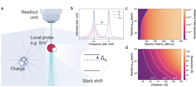
a The local probe is an optically active atomic defect with non-linear Stark-sensitive energy levels. The read-out unit is a photoluminescence excitation spectroscopy microscope. b A nearby charge shifts the optical transition from C0 to Cs by Δs(r) depending on its distance r. Additionally, an ensemble of remote fluctuating charges broadens the signal from Cs to Cs,b, depending on the charge density ρtrap. c Relative electric field sensitivity ∣ΔE∣/E to electric field changes as a function of electric field Es and trap density ρtrap. Left of the white dashed line, Stark-shifts are not large enough to be resolved by the Rayleigh criterion. Larger field strengths are correlated with larger inhomogeneous broadening. Eq. (1) assumes Δμ = 6.1 × 10⁻⁴ GHz/(MV/m)2, Δα = −5.1 × 10⁻⁵ GHz/(MV/m)2, Δβ = −5.5 × 10⁻⁸ GHz/(MV/m)3 and Δγ = −2.2 × 10⁻¹⁰ GHz/(MV/m)435. d The sensor’s resolution in determining the distance of an elementary charge based on differentiating two distinct charge traps as a function of the charge trap density and distances. The resolution was determined for a trap with variable distance r and a bias field equivalent to a trap distance of 0.8 nm. The dashed white lines indicate the inscribed resolution thresholds.
The read-out unit is a microscope which is used to perform photoluminescence excitation spectroscopy on the local atomic probe, and therefore does not require magnetic resonance methods5. Measuring the energy shift reveals the magnitude of the electric field at the sensor probe Es via the DC-Stark-shift
with Δμ the change in the dipole moment and Δα, Δβ, and Δγ the differences between the higher-order polarizabilities35. Importantly, in contrast to non-inversion symmetric configurations of color centers, such as the nitrogen-vacancy center in diamond36 and the silicon-vacancy center in silicon carbide37, the negligible linear- and strong non-linear response due to inversion symmetry makes the sensor applicable to typical semiconductor dopant and defect densities. If Δα dominates and the observed ΔStark arises from a localized elementary charge e at a distance r from the sensor, then
Decreasing distances of charges to the sensor causes increasingly higher spectral shifts. This characteristic makes sensors that have an inversion center remarkably sensitive to charges in close proximity and insensitive to electric field background noise.
The ~10−7 relative electric field sensitivity (Fig. 1c) allows for a spectral sensor read-out that provides exceptionally high spatial resolution, reaching down to a few Ångström, even for charge densities up to 100 ppm (Fig. 1d).
In this work, the SnV local probe is stationarily located inside a bulk crystal housed in a cryostat at 4 K, however, it could also be integrated into the tip of a scanning probe microscope38 for position dependent measurements well established in magnetometry39,40 or into a nanodiamond for integration with other materials41 or even biological samples42. Alternatively to the SnV, also other D3d symmetric defects, such as the silicon-29 or germanium-vacancy30,43 and other inversion symmetric defects in other materials, for example, in silicon44, could be applied as a local probe. To demonstrate the non-linear sensor principle, we utilize a single SnV that was created upon ion implantation and annealing.
Results
Determining charge trap positions at the atomic lattice scale
The electrometer and its environment are depicted in Fig. 2a. To demonstrate its sensing capability, we analyze the time-varying quasi-static electric field that is caused by charging and neutralization of crystal defects in the surrounding lattice under laser irradiation45,46. Using the recorded field magnitude at different configurations of the charge distribution, we can resolve the surrounding crystal defects at the lattice scale.
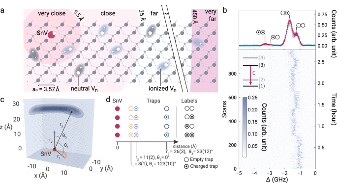
a Illustration of a diamond lattice including SnV and defects, identified as multi-vacancy complexes (Vn). Charges localized in these traps induce a Stark-shift of the energy levels of the atomic sensor probe. From very close to far, respectively, the spectral impact of an elementary charge can be categorized as follows: Spectral shifts larger than 30 GHz are detectable by photoluminescence spectroscopy, spectral shifts of ~GHz are detectable by photoluminescence excitation spectroscopy (PLE), and inhomogeneous broadenings are detectable by PLE. Charges in the very far region have negligible effects. b Top: An integrated multimodal PLE spectrum recorded with the SnV sensor S1 (blue) and modeled with Monte-Carlo simulations (red, error bars represent statistical standard deviation) to identify a proximity charge trap configuration (states labeled above the peaks, ⊙ and ○ represent ionized and neutral traps, respectively) and the surrounding charge density. Bottom: Time-resolved individual linescans. Inset: SnV level scheme and the probed transition. c Left: Identified charge trap configuration corresponding to (d), their relative positions and their probability distribution with respect to the SnV probe. Distributions resemble a donut shape due to the direction-independent calibration of the sensor. RIGHT: Table indicating the charge states and position of the identified traps.
If all traps are neutral, the total field at the position of the probe is zero, and the optical transition of the SnV is unperturbed. A charged trap will induce an electric field , which Stark-shifts the optical transition energy according to Eq. (1). If a single elementary charge is located in proximity to the probe, the C transition is shifted more than its own linewidth, producing a spectral jump. (Fig. 1b). The magnitude of the spectral shift can be determined by comparing with the unperturbed case; adding both resonances in one spectrum leads to a unique optical fingerprint with two peaks.
To collect the spectra, we measure the fluorescence from the C transition of the sensor S1 under photoluminescence excitation (PLE) with a narrowband laser (Fig. 2b). The experiment is conducted under 0.5 nW (a power much below the expected saturation power47 for excluding power broadening effects) of 619 nm resonant light. Additionally, a 2 μW (CW power) 450 nm 4 ms pulse is applied between line scans for SnV charge state reinitialization. From the spectral shift, we extract the charge-induced electric field. Knowing the local field and using the polarizability enables us to estimate the trap-probe distance.
For N charged traps in the probe’s vicinity, the electric fields add up to and the individual charges cannot directly be separated. To distinguish the 2N charge states, the Stark-shifted PLE spectra are recorded repeatedly. Due to laser irradiation, the traps will be ionized and neutralized randomly. By sampling a large set of configurations complex trap distributions can be analyzed.
In addition to nearby charges that cause significant spectral line shifts, the numerous randomly distributed traps in the distant surroundings also contribute. These traps exhibit fluctuating charge states, resulting in a fluctuating electric field that causes inhomogeneous broadening. Consequently, the density of charge traps ρtrap within the lattice can be determined using linewidth measurements. We find that traps can be resolved with subnanometer resolution. For trap densities ρtrap ≈ 0.3 ppm, detection volumes of 1503 Å3 are feasible. Fluctuating charge traps at larger distances primarily contribute to inhomogeneous broadening.
Finally, to fully calibrate the electrometer, we consider its non-linear response to external fields, causing an interdependence of the different external field components. For example, the effective Stark shift induced by two charges does not equal their sum. This phenomenon enables high resolution but makes the analysis of recorded fingerprints highly complex. We therefore build a theoretical database of simulated spectra for a large variety of discrete proximity charge positions and remote trap densities using Eq. (1).
We now analyze the complex experimental four-peak fingerprint from Fig. 2b quantitatively. We use experimentally determined polarizabilities35. By comparing experimental and simulated fingerprints, we find several possible trap configurations. From these possible configurations, we identify the most plausible by specific physical considerations (Supplementary Fig. 3).
The most likely configuration of nearby traps consists of a permanent Ebias, generated, for example, by a permanently ionized trap, and two additional traps inducing spectral jumps. We assign labels to the spectral peaks in Fig. 2b based on the charge state of the two additional proximity traps {○○, ○⊙ , ⊙○, ⊙⊙}, where ○ signifies an uncharged trap, and ⊙ a charged trap. Subsequently, we determine the position of these charge traps up to an azimuthal angle using Monte-Carlo simulations. We extract the relative Stark-shifts corresponding to the proximity trap distances r1 = 8(1) Å, r2 = 11(2) Å, r3 = 26(3) Å (Fig. 2c, d) and a remote trap density of 74(22) ppm. Furthermore, we find for two charges, azimuthal angles with θ1 = 123(10)° and θ3 = 23(12)°. The polar angles cannot be further confined because of the cylindrical symmetry of the problem setup.
Charge dynamics
For identifying the positions of charge traps, we have used accumulated spectral fingerprints that reflect the integrated spectrum for the entire set of charge states. However, understanding time-resolved charge transfer dynamics requires comparing individual read-out events of our electrometer and, therefore, single PLE linescans. We interpret the charge state changes with a simplified charge transfer picture (Fig. 3a): Charge traps, later identified as multi-vacancy complexes Vn, can be ionized under laser illumination through two distinct processes: negative charging, which occurs when the trap captures an electron promoted from the valence band leaving a positively-charged hole in the band; and positive charging when an electron is promoted from the trap to the conduction band. Generated holes and promoted electrons then diffuse and recombine with other charge traps, leading to an overall charge-neutral environment. We denote the event ○ → ⊙ as ionization and the inverse ⊙ → ○ as neutralization event. The charge transfer picture4,48 is consistent with the autocorrelation measurements we performed on the sensor emission (Supplementary Fig. 6).
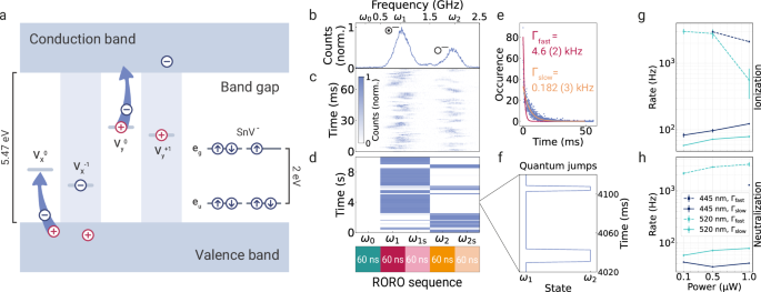
a Illustration of an SnV, ionized () and neutral () defects, i.e., the charge traps, in the diamond bandgap. Ionization occurs when either an electron is promoted from the valence band to the charge trap or an electron is promoted from the trap to the conduction band by laser irradiation. Neutralization occurs when the trap either catches a hole from the valence band or an electron from the conduction band. b Integrated PLE spectrum and c time-resolved linescans acquired by the SnV sensor S2. d Using the specific resonance for each charge state obtained from the PLE spectrum, the laser frequency is periodically switched between the off-resonant ω0 and the resonances ω1, ω2. Each resonance is probed in two 60 ns steps with an additional frequency offset to compensate for spectral diffusion. The entire rapid optical readout (RORO) sequence takes 300 ns. Counts registered during each acquisition step are analyzed to determine how long a particular resonance remains bright. e An example histogram of the bright times of the resonance ω1 before a spectral jump to ω2 occurred. The data is fitted with a bi-exponential function that has two rates with constants Γfast and Γslow. f A zoom-in of the spectral jumping plot from subfigure d reveals fast quantum jumps occurring on the order of ms. g and h To investigate the influence of photon irradiation energies on the recharging dynamics, spectral jumping rates are acquired under distinct laser wavelengths and powers. Rates are extracted separately for the investigated nearby trap’s spectral jumping directions corresponding to ionization (redshift) and neutralization (blueshift) processes. Dark blue data points are acquired under 445 nm and green data points under 520 nm laser illumination. For each wavelength, the measurement is repeated at three different powers. Data points connected by solid lines correspond to the extracted Γslow exponential rate constant. Fast rates Γfast are connected by dashed lines and shown for histograms in which a fit to a bi-exponential distribution was possible. The error bars represent 95% confidence intervals extracted from the fits.
To showcase the characterization of a local charge environment and dynamics of the charge transfer processes, we acquire a high timing-resolution set of data from a second sensor S2. The temporal analysis of the data acquired from S1 is provided in the supplementary materials. S2’s charge dynamics are dominated by a single spectral jump, as shown in Fig. 3b. We label the two states as the neutral ○ and ionized ⊙ states following our previous description.
The individual lines in Fig. 3c are acquired with a GHz/μs scanning speed by using a chirped frequency modulation of an EOM-generated sideband of a narrowband laser.
After identifying the resonance peaks in the integrated spectrum using the chirped frequency modulation, we perform a rapid optical read-out (RORO) of the charge trap (Fig. 3d). We generate a readout sequence by repeatedly modulating the sideband targeting five frequencies with 60 ns acquisition steps: off-resonant ω0, the peaks of two resonances ω1,2 and some pre-selected frequency offset ω1s,2s to probe the resonances even if some spectral diffusion has taken place. The entire RORO sequence lasts a total of 300 ns. Using a single-shot read-out sequence, we extract a specific charge state of the sensor. We then visualize the distribution of duration the sensor stayed on one of the resonances in a histogram, as exemplified for the first resonance ω1 in Fig. 3e. The histograms are fitted with a bi-exponential distribution featuring two charge transfer rates Γfast and Γslow, reflecting slow and fast charge dynamics as detailed below.
To analyze the charge dynamics on the shortest time scale available in the specific measurement configuration, we zoom into the data of Fig. 3d and look closely at the quantum jumps (as shown in Fig. 3f). We observe that although a time period can look bright on the scale of seconds in Fig. 3d, faster jumps occur on the millisecond scale. We further investigate the source of the bi-stability of the rates by selectively analyzing windows from an extended dataset acquired under the same conditions as in Fig. 3d. We find that if a time interval is predominantly bright for one resonance, the jumping rate from that state is closer to the extracted slow rate. For example, a predominantly bright time window of a total of ~31 s for ω1 yields a jumping rate 26(5) Hz. On the other hand, when the time interval seems mainly dark, the jumping rate decays quicker, e.g., during a predominantly dark time window of ~13 s for ω1 yields 1.91(13) kHz. While identifying the underlying physical process of the rate change requires further investigation, one possible explanation could be the change of a distant charge donor’s trap state. The rate of the spectral jump may be modified by the availability and quantity of the required free charged particles.
To further experimentally investigate the origin of the charge dynamics, we repeat the measurement with a second laser applied during the off-resonant part of the readout sequence to characterize the charge dynamics induced by the properties of the illumination. Ultimately, such a measurement allows us to spectroscopically investigate the local charge environment and, more specifically, how its dynamics are influenced by external laser irradiation or other sources of noise in the nanoscopic local environment. We investigate six conditions: for both 445 and 520 nm wavelengths, three laser power levels are set. We plot the extracted rates for ionization and neutralization processes, respectively, in Fig. 3g and h.
An interesting and at first sight unexpected observation is made that the neutralization process is observed. Green illumination induces faster jumps than the higher energy blue illumination. This may be caused by a two-photon process involving a defect level within the bandgap that is more likely to interact with the green laser than direct ionization from or to the valence and conduction bands. Acquiring data at additional power levels, illumination wavelengths and conducting measurements on different emitters with varying trap environments would enable extending this proof-of-principle experiment to a more detailed study.
Given the exceptional timing resolution of our RORO method, we can determine charge processes exceeding kHz rates, which are orders of magnitude faster than the typical ~1 Hz modulation rates of tunable lasers. Using conventional PLE by applying a voltage signal is not quick enough to observe the charge dynamics in the sample. Moreover, RORO could reveal charge processes with several MHz rates by utilizing the 60 ns minimum read-out steps. Reaching this limit requires estimated photon detection rates of ~17 MHz. By further reducing emitter lifetimes, for example through the Purcell-enhancement by cavity integration, the 60 ns read-out resolution could be reduced to several nanoseconds (see Supplementary Table I).
Evaluating spectral diffusion
The charge transfer-induced spectral dynamics are highly detrimental for quantum technological applications. Spectral diffusion, a term indicating the probabilistic nature of the observed spectral dynamics, leads to optical decoherence23,24,25,26, which results in reduced entanglement fidelity in quantum network nodes27,49.
Knowing the non-linear receptiveness of our quantum electrometer to charge-noise, we now make predictions of how a specific charge distribution influences the spectral properties of a color center. Based on our model, we provide an overview of the inhomogeneous broadening caused by a certain charge trap density ρtrap. The details of the calculation are provided in supplementary information.
We first focus on the bulk case (Fig. 4a) and then analyze surface charge traps () for two different surface geometries, planar (Fig. 4b) and cylindrical (Fig. 4c). We find that an implantation depth of d > 21 nm and a cylinder with a radius of r > 45 nm will warrant that surface charges do not deteriorate the spectral properties of an SnV color center with linewidth broadening of <1%. Such broadening leads to 90% interference visibility and more than 87% entanglement fidelity49. Similar estimations can be performed for any defect given a known polarizability. Control measurements concerning spectral diffusion with respect to the illumination field are provided in the supplementary information.
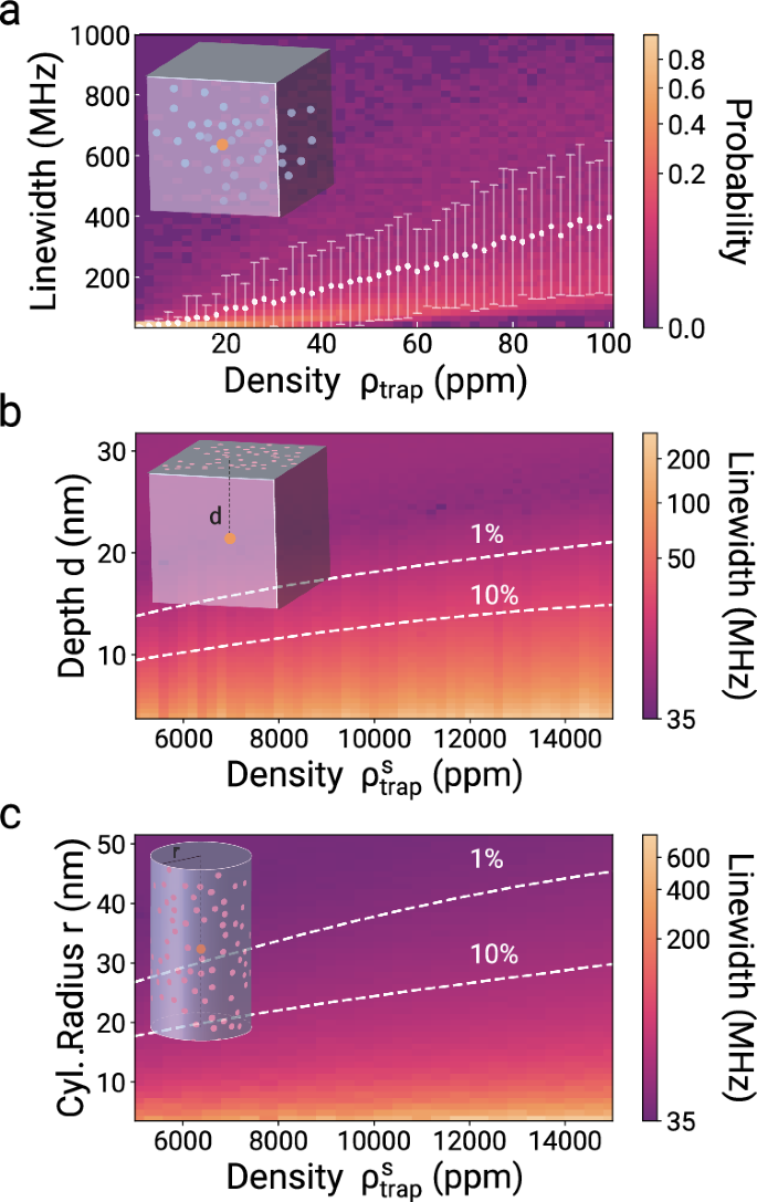
a Inhomogeneous broadening of an SnV with a lifetime-limited linewidth of 35 MHz as a function of ρtrap in units of ppm in bulk diamond. The colors indicate the linewidth distribution. The mean and variance of the distribution are shown by the white dots and error bars. b Inhomogeneous broadening as a function of the distance of an SnV to a planar surface and the surface trap density defined as a fraction of surface lattice sites. The dashed lines show the threshold of 1% and 10% of broadening compared to the lifetime-limited linewidth of 35 MHz. c Inhomogeneous broadening of an SnV centrally located in a cylinder with radius r as a function of . The dashed lines signify 1% and 10% broadening.
The estimated minimum detrimental distances make SnVs and similar color centers well suited for the integration into nanostructures that enhance photon collection efficiencies50 and provide tailored emission properties via the Purcell-effect51,52 for quantum information applications.
It must be noted that an increase in the absolute lifetime limited linewidth due to the Purcell effect would decrease the depth and radius criteria. Furthermore, these analyses do not take band-bending and Fermi level modification effects into account, which could have additional implications on the charge state stability and brightness of the color centers.
Identifying material properties: divacancy formation
Based on the electrometers ability to quantify charge trap densities, we extend our investigation of material properties and combine our sensor data with additional simulations to answer further open research questions. Specifically, we determine the physical origin of charge traps in implanted diamond. Considering a sample with <1 ppb of nitrogen and boron, and even lower lattice defect concentrations53, the estimated charge trap density of 74(22) ppm must originate from the Sn-ion implantation damage and the subsequent annealing process. Implantation of ions produces Frenkel pairs: a pair of one monovacancy V1 and one dislocated interstitial carbon atom. During annealing V1 becomes mobile and can form vacancy complexes, a process not well understood and an active area of research54,55,56 (Fig. 5a).
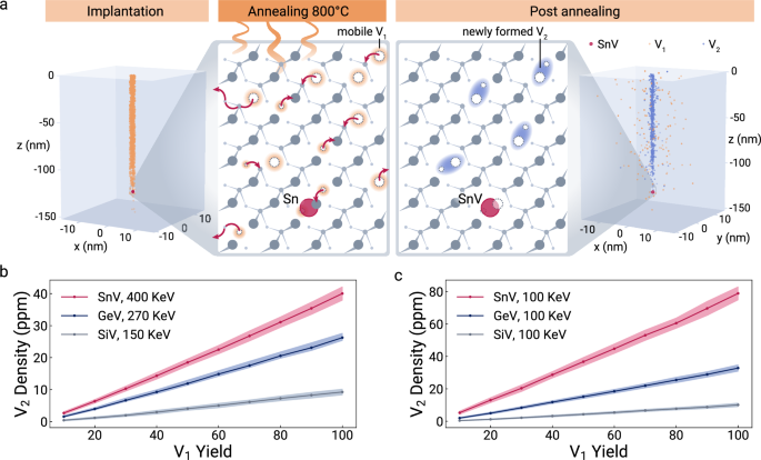
a Implantation panel: Spatial distribution of created monovacancies (V1) by 400 keV Sn implantation predicted by SRIM67 simulations. Annealing panel: V2 formation during annealing at 800 °C. At elevated temperatures, V1 start diffusing. Then, V1 immobilize either by moving to the boundaries, recombining with interstitial carbons, or forming V2. Post annealing panel: Distribution of V1 and V2, which are distributed in the vicinity of the damage channel caused by the Sn implantation. Zoom in: V2 in the vicinity of the SnV. b Simulated densities of V2 as a function of the V1 implantation yield (% of participating V1 estimated by SRIM simulations) for the three different species Sn, Ge, and Si. A reduced V1 yield is attributed to recombination with interstitial carbons. The implantation energies are selected so that an average implantation depth of 100 nm is reached. c Densities of V2 for 100 keV implantation energy. The error bands represent the statistical standard deviation.
Here, we estimate the V1 to divacancy V2 conversion yield using a kinetic Monte-Carlo simulation57 in combination with a simple stochastic diffusion model described in the supplementary information.
We consider the V2 density as a proxy for higher-order vacancy complexes Vn. Annealing up to 1100 °C primarily converts V2 into V3 and V454,58. We indeed observe wavelength-dependent spectral diffusion and jumps (Supplementary Fig. 10), indicating different ionization energies of the multiple trap species. We interpret the estimated density of V2 as both an order-of-magnitude approximation and an upper limit for the overall charge trap density. We estimate and compare ppm to the experimentally estimated trap density of ppm. Due to charge neutrality, the overall charge density would correspond to twice the density of V2 with = 80.0(4.2) ppm. We attribute the small mismatch to a reduction in the density of the Vn compared to the V2 estimation.
Understanding the origin of the charge traps also provides a clear path on how to create optically noise free group-4 vacancy defects in diamond. Single-peak fingerprints, indicating a low Vn density, are more frequently observed in high-pressure high-temperature (HPHT) annealed samples at 2000 °C48, which is in agreement with electron spin resonance measurements58.
Spectral jumps have been reported before for group-4 vacancy defects47,59,60. Comparing the Vn density for the atomic species Si, Ge, and Sn and varying implantation energies (Fig. 5b, c) indicates that Si implantation leads to the lowest V2 density. This observation is in accordance with the more frequent reports of spectrally stable SiV61 compared to SnV, now explained with our analysis that heavier ions cause increasing Vn densities.
Discussion
In conclusion, we use the SnV in diamond, a representative of an inversion symmetric point defect in wide-bandgap materials, as a local probe to detect localized charges with Angstrom resolution at the lattice scale. For this work, we constrained some degrees of freedom in the positions of the traps for the Monte Carlo simulation to make it more time-efficient. The main constraints were the confinement of the remote charges to a conical volume z > z0, where z0 is the assumed implantation depth of the SnV. The conical volume modeled the lattice damage remaining after annealing. Furthermore, we confined the three charge traps responsible for the multimodal spectrum to a plane. These limitations are not fundamental to this method and can be relaxed. In principle, a more extensive parameter space can be explored, but this would require significantly longer simulation times and increased memory demands. The addition of a more in-depth calibration of the probe would ameliorate this shortcoming. Particularly, implementing a probe-specific multi-directional calibration process, with the inclusion of extracting direction-dependent polarizability coefficients, would allow us to construct suitable polarizability tensors. Using such a calibrated probe in combination with the Monte Carlo simulations would help enable azimuthal localization for full positioning. Alternatively, correlated sensing15,16 can be used to reduce the uncertainty of the charge traps’ absolute position in our work.
We utilize a rapid spectroscopy technique based on frequency modulation with electro-optical modulators, to enable time-resolved access for recording and measuring charge dynamics of single nonfluorescent defects under laser irradiation with MHz readout rates, demonstrating a time-resolved quantum electrometer working at the atomic scale (see Table 1). Such observations on the single-charge scale open the possibility to further understand the origin and type of charge defects and charge transport phenomena. Intriguingly, a sensor such as the one proposed in this study can be used to study topological quantum phenomena of ferroelectrics, for example, the detection of ferroelectric vortices or polar skyrmions62.
An exciting secondary application is to use our sensor for sub-diffraction resolution position estimation. The electrometer’s sensitivity to background charge-noise can be used to sense the position of an illumination laser with sub-diffraction precision. We estimate that a resolution below 1 nm can be achieved (Supplementary Fig. 8).
From the analysis of the local charge environment, we are able to understand the nanoscopic origin of spectral diffusion of SnVs and formulate mitigation strategies. We identify that the local defect density of Vn should be reduced, and quantify precisely the maximally allowed charge trap density for reaching optical coherence.
Building on the insights of our work, we believe that our electrometer opens up an exciting direction in material science, enabling the time-resolved study of single elementary charges with Ångström spatial and 100 ns temporal resolution.
The integration of the sensor into a scanning-probe tip or a nanodiamond will allow for the study of single and multiple lattice defects in silicon transistors, optically active quantum memories, and defect-induced charge-noise in on-chip ion and superconducting computers, potentially mitigating these detrimental effects and contributing to the further optimization of materials for the application in quantum technology.