Article Content
1 Introduction
Ablation using ultrashort laser pulses has been widely applied in laser processing [1], surface texturing [2], and welding [3]. Understanding the ablation dynamics through experimental observations is crucial for controlling these phenomena and laser parameter optimization [4]. High-speed cameras, such as charge-coupled device (CCD) and complementary metal-oxide-semiconductor (CMOS) cameras, are commonly used for imaging on a timescale of hundreds of nanoseconds to milliseconds [5, 6]. Time-resolved pump-probe imaging is typically employed for imaging on femtosecond to nanosecond timescales [7, 8]. This technique requires repetitive measurements with varying delay times to capture the phenomena temporal evolution, making it unsuitable for irreproducible or difficult-to-reproduce dynamics. Consequently, ultrafast ablation dynamics analysis has been limited to conditions in which reproducibility can be ensured.
Meanwhile, the increasing laser parameter diversity, such as double pulses [9, 10], burst pulses [11, 12], spatial shaping [13,14,15,16], and ultrahigh intensities [17], along with the expanding range of target materials, including brittle materials [18], composites [19], polymeric materials [20], and biological tissues [21], has created a growing demand for the ability to understand and control complex ablation dynamics where reproducibility cannot always be ensured. To enhance the performance and expand the applicability of laser ablation technologies, it is necessary to achieve the single-shot imaging of spatiotemporal dynamics across a wide range of ablation phenomena.
Recently, several ultrafast single-shot imaging techniques have been developed for femtosecond-to-nanosecond timescales [22, 23], including sequentially timed all-optical mapping photography (STAMP) [24], compressed ultrafast photography [25], frequency recognition algorithm for multiple exposures [26], single-shot noncollinear optical parametric amplification imaging [27], and swept coded aperture real-time femtophotography [28]. Among them, STAMP shows promise for visualizing complex ablation dynamics with high spatiotemporal resolution because it avoids the image quality degradation that is often associated with spatial frequency sacrifices or image reconstruction processes. However, examples of laser ablation dynamics visualization using STAMP remain limited.
Two major factors limit the compatibility of STAMP with a wide range of laser ablation systems. First, existing STAMP systems are typically complex and bulky, and are often mounted on optical tables in a fixed setup. This complexity results in time-consuming construction and alignment, which hinders the flexibility required for widespread adoption across different setups. To promote the visualization of diverse phenomena, it is essential to make the system more compact and portable, thereby enabling easier integration into various experimental environments.
Second, STAMP has traditionally required broadband light sources, such as femtosecond Ti:sapphire lasers (800 nm center wavelength and ~ 30 nm bandwidth), to achieve high temporal resolution and capture a large number of frames. However, to adapt STAMP to a wider variety of laser systems, including relatively narrow-bandwidth femtosecond Yb-based lasers, it is necessary to address its dependency on broadband light sources. Several spectral broadening techniques have been developed, including gas-filled hollow-core capillaries [29], photonic crystal fibers [30], and thin solid plates [31, 32]. Thin solid plates offer a compact and stable approach to spectral broadening. Addressing the system’s complexity and its dependence on broadband light sources will significantly improve its compatibility with a wider range of laser ablation systems, making it a more versatile tool for ultrafast imaging.
In this paper, we present a compact and portable STAMP system that incorporates thin-plate-based spectral broadening. The system consists of three independently packaged modules. This portable design can be easily integrated into existing time-resolved pump-probe imaging setups, transforming them into ultrafast single-shot imaging systems. The capability of the system was demonstrated by integrating the developed STAMP modules into a pump-probe system using a Yb:KGW laser, following initial demonstrations of ultrafast imaging with a Ti:sapphire laser system.
2 System development
2.1 Overall system
The developed STAMP system enables ultrafast sequential image acquisition when integrated into narrowband pump–probe imaging setups, as shown in Fig. 1. The system consists of three main modules: a spectral broadening device (SBD), temporal mapping device (TMD), and spatial mapping device (SMD). The system is packaged into three independent modules using a compact and stable optical technique for each module. This modular design allows the system to be removed from the optical table and transported to other laser systems while minimizing the misalignment of optical components.
During operation, an ultrashort pulse is spectrally broadened by the SBD and then time-stretched by the TMD. The pulse reaches the target at different times for each wavelength. Subsequently, the SMD spatially separates the different wavelength bands and projects them onto different areas of the image sensor, resulting in the acquisition of ultrafast sequential images.
The system was designed to operate at wavelengths of approximately 515 nm, corresponding to the second harmonic of Yb-based lasers. This second harmonic is often used in pump-probe imaging with Yb-based lasers, where a fundamental wavelength of approximately 1030 nm serves as an ablation pulse. Using the second harmonic as the probe pulse instead of the fundamental harmonic helps reduce the noise in image acquisition caused by scattering of the ablation pulse. We developed three STAMP modules to achieve single-shot imaging when integrated into pump-probe setups.
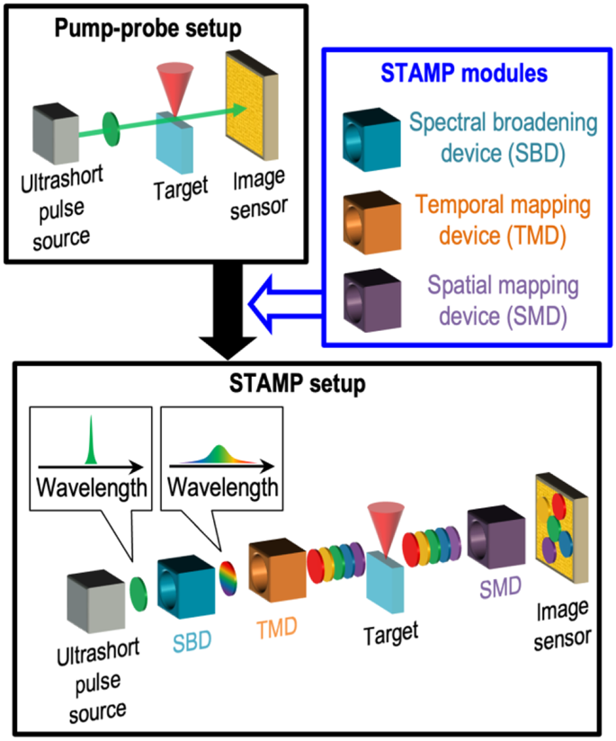
Schematic of the developed STAMP system for integration into pump-probe imaging setups
2.2 Spectral broadening device (SBD)
The SBD module broadens the ultrashort-pulse light source spectrum, achieving sufficient bandwidth for use as a probe in STAMP. Spectral broadening methods for ultrashort pulses include gas-filled hollow-core capillaries [29], photonic crystal fibers [30], and thin solid plates [31, 32]. Stable and easy integration of gas-filled waveguide-based methods into STAMP is challenging owing to timing fluctuations caused by gas pressure variations and the complexity and bulkiness of the vacuum setup. Photonic crystal fibers are highly sensitive to the directionality of the input pulse, which complicates the alignment and introduces temporal instability in the beam, posing similar challenges for STAMP integration. By contrast, the thin-plate-based method overcomes these challenges by offering compact and stable spectral broadening, making it a promising choice for this application. In this study, we implemented thin-plate-based spectral broadening in the STAMP system.
Figure 2a and b show a schematic of the optical layout and a photograph of the constructed SBD module, respectively. A CaF2 plate [32] was used as the thin plate. A 3-mm-thick CaF2 plate was placed near the focal point of a relay lens system consisting of lenses with focal lengths of 150 and 50 mm. The incorporation of the two irises enabled the precise introduction of an ultrashort pulse into the module. The module was mounted on an optical rail and fitted within dimensions of 100 × 500 mm. Further spectral broadening can be achieved using multiple plates in the module.
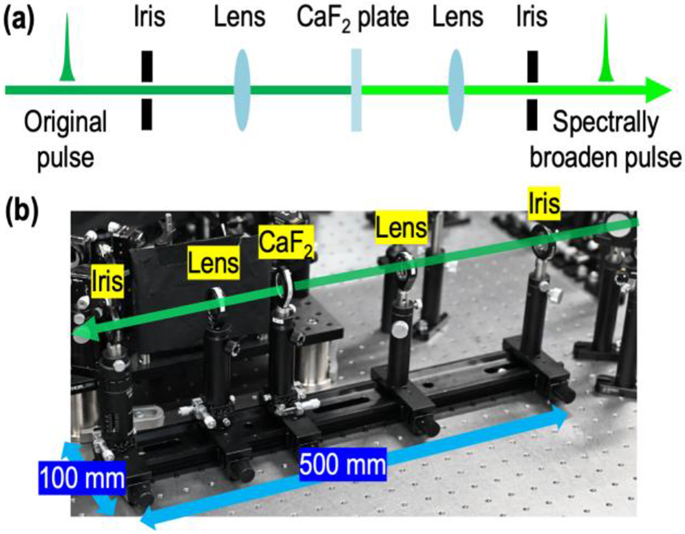
Spectral broadening device (SBD). (a) Schematic of the optical layout. (b) Photograph of the constructed module
2.3 Temporal mapping device (TMD)
The TMD stretches the pulse according to the required imaging timescale. Techniques such as glass rods or glass blocks are commonly used for femtosecond timescales [24, 33], while either a grating pair or a prism pair is employed for picosecond timescales [24]. For sub-nanosecond to nanosecond timescales, methods such as free-space angular-chirp-enhanced delay [34], spectrum circuits [35], and spectrum shuttles [36] are used. In this study, we developed a compact TMD that can adjust the imaging timescale from picoseconds to nanoseconds by switching between a grating-pair configuration and a spectrum-shuttle configuration. The grating pair is used for picosecond timescales, whereas the spectrum shuttle, implemented by adding mirrors to the grating pair, extends the timescale to the nanosecond range. This flexible switching capability within a single device enables the TMD to cover a broad timescale range, thereby enhancing its versatility and compactness for various ultrafast imaging applications.
Figure 3a and b show a schematic of the optical layout and a photograph of the constructed TMD module, respectively. The incident pulse is aligned to pass through the two irises. The pulse is directed into the grating pair using flipper-mounted mirrors after its polarization is adjusted for maximum diffraction efficiency using a half-wave plate. In the grating pair, the pulse is dispersed by two diffraction gratings (G1: GH50-24 V; G2: GH25-24 V; Thorlabs, US), reflected by a mirror (M1: BBSQ2-E02; Thorlabs, US), and returned along the initial incoming path before being extracted by a 50:50 beam splitter (BS013; Thorlabs, US). During this round trip, a time delay is introduced for longer wavelengths based on the optical path difference, resulting in a stretched pulse. This grating pair stretches the pulse to a maximum duration of ~ 400 ps in the 515-nm wavelength band. Further pulse stretching is achieved by converting the setup into a spectrum shuttle by adding two mirrors (M2 and M3) between G2 and M1, which produce spectrally separated burst pulses at intervals ranging from 50 ps to 2 ns. The stretched pulse is coaxialized with the incident pulse to the module and exits the module. The module, mounted on a breadboard, has dimensions of 200 × 250 mm.
2.4 Spatial mapping device (SMD)
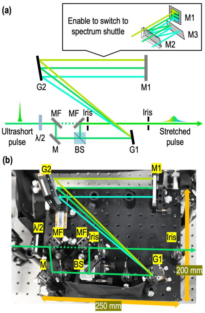
Temporal mapping device (TMD). (a) Schematic of the optical layout. (b) Photograph of the constructed module. λ/2: half-wave plate; M: mirror; MF: mirror mounted on the flipper; M1–M3: Mirrors 1–3; BS: beam splitter; G1 and G2: diffraction gratings 1 and 2
The SMD spatially separates the spectral components that pass through the target at different times and images them in different areas of the image sensor. Various methods can be employed in the SMD, including spectral filtering [37], slicing mirrors [38], and lens arrays [39]. A system using slicing mirrors requires a larger number of optical elements, resulting in a complex setup, while a system using lens arrays suffers from a lower spatial resolution. By contrast, a spectral filtering system offers a simple setup with only a few optical elements and achieves high spatial resolution. Based on these considerations, we chose a spectral filtering system for the SMD.
Figure 4a and b show a schematic of the optical layout and a photograph of the constructed SMD module, respectively. The module consists of an iris to adjust the field of view, a diffractive optical element (DOE) to divide the pulse into multiple frames, a bandpass filter (BPF) to transmit different wavelengths depending on the angle of incidence, and a lens for imaging purposes. The DOE (DE-R 352; HOLOEYE, DE) generates a 4 × 6 dot beam array with a full diffraction angle of 12.6° at a wavelength of 515 nm. The BPF (532.0–1 OD6; Alluxa, US) has a center wavelength of 532.0 nm and a bandwidth of 1 nm. The imaging lens (AC254-045-A; Thorlabs, US) has focal length of 45 mm. A blocker is positioned after the imaging lens to eliminate the zeroth-order beam passing through the DOE. The module, mounted based on a cage system, fits within dimensions of 100 × 150 mm. This module was designed to fit the image sensor with a 13.3 × 13.3 mm imaging area (ORCA-Flash4.0 V3; Hamamatsu Photonics, Japan), as used in this study. An additional BPF (FBH520-40; Thorlabs, US) was mounted on the image sensor to reduce the noise caused by emissions from ablation and background light. The DOE azimuthal angle was optimized to 14° to minimize the standard deviation of the wavelength intervals between frames. As shown in Fig. 4c, the central wavelengths for each frame are distributed at an average interval of 0.67 nm. This setup enables the single-shot acquisition of 24-frame images, using the probe’s 16-nm bandwidth. The standard deviation of the wavelength differences between consecutive frames was reduced to 0.25 nm while remaining non-uniform. This wavelength interval non-uniformity contributes to non-uniform time intervals, which must be considered in the analysis of phenomena using STAMP, such as velocity or transmittance changes. Additionally, spectral overlap occurs between adjacent frames because each frame has a 1-nm bandwidth, which exceeds the average wavelength interval of 0.67 nm. However, almost no overlap was observed when every other frame was considered. The minimum exposure time, defined by the Fourier-limited pulse duration [37], was 390 fs, which represents the temporal resolution limit in this SMD. When pulse stretching occurs owing to the TMD, the exposure time increases.
Here, we describe the development of a STAMP system that incorporates thin-plate-based spectral broadening and is packaged into three compact and portable modules. This design addresses the reliance on broadband light sources and mitigates the challenges of time-consuming construction and alignment, thereby enabling seamless integration with narrow-bandwidth femtosecond Yb-based lasers. This facilitates the visualization of various ultrafast phenomena induced by Yb-based lasers.
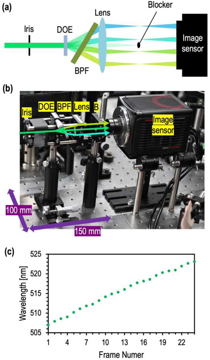
Spatial mapping device (SMD). (a) Schematic of the optical layout. (b) Photograph of the constructed module. (c) Center wavelengths for each frame. DOE: diffractive optical element; BPF: bandpass filter; B: blocker
3 Experiments
3.1 Ultrafast imaging of laser ablation
Using the developed STAMP modules described in Sect. 2, we demonstrate the ultrafast imaging of laser ablation with a Ti:sapphire-based system. The experimental setup is illustrated in Fig. 5a. A mode-locked Ti: sapphire laser with a chirped-pulse amplification (CPA) system (Astrella-USP-1 K; Coherent, US) was used as the light source. The system generates laser pulses with a center wavelength of 800 nm, bandwidth of 35 nm, and pulse duration of 35 fs. A fundamental pulse was used for ablation. After being delayed by a delay line, the pulse was focused onto a 50-µm-thick glass plate using a lens with a fluence of 18 J/cm2. The pulse was removed using a mechanical shutter (SH05R; Thorlabs, US).
An ultrashort pulse for imaging was generated from the same source pulse using an optical parametric amplifier (OPA) (OPerA Solo system; Coherent, US). As shown in the spectra obtained using a spectrometer (GREEN-Wave-VIS; StellarNet, US) (Fig. 5b), the generated pulse has a center wavelength of 515 nm and a bandwidth of 11 nm, and the SBD successfully broadens the bandwidth to 25 nm. The pulse stretched by the TMD was focused onto the target using a condenser lens with a focal length of 40 mm (AC254-040-A; Thorlabs, US). After passing through the target, the pulse is magnified using an objective lens (GLI-PLACH10XLM; Wraymer, Japan) and imaged on the image sensor through the SMD. The time intervals were calibrated by adjusting the optical delay line between the ablation and probe pulses to determine the position where filamentation inside the glass was observed in each frame. The average time interval between frames was 15 ps. Based on this, the group velocity dispersion introduced by the TMD was calculated to be 22 ps/nm, resulting in an exposure time (i.e., temporal resolution) of 22 ps.
The imaging results are shown in Fig. 5c. For enhanced contrast, the luminance values of the images captured during ablation were divided by those captured before ablation. After irradiation with an ablation pulse, rapid filamentation occurred inside the glass. However, no significant changes in the filament shape were observed until 341 ps. The striped pattern of the filament is attributed to the spatial profile degradation of the ablation pulse emitted from the OPA, resulting in a focused beam with multiple intensity peaks. By contrast, in air, plume expansion from the glass surface was observed, progressing approximately 15 μm at 341 ps. The expanding plume exhibited a textured structure caused by the spatial profile of the ablation pulse, and its structure gradually changed during propagation. Understanding the plume propagation dynamics is crucial for laser processing involving double [10] or burst pulses [12], as the plume’s spatiotemporal profile significantly affects these processes. Based on the plume dynamics analysis, our developed STAMP system can provide fundamental insights into a variety of Yb-based laser processing phenomena.
In this study, the time window was set to 356 ps as an example to visualize the gradual changes across the 24 frames achieved using a grating pair to stretch the pulse. This setup provides a clear demonstration of the ultrafast imaging capabilities for observing the plume expansion dynamics. Beyond 341 ps, the plume is expected to continue expanding, with its transmittance gradually changing and shockwaves forming in the 500 ps–1 ns range [36]. By switching to a spectrum shuttle and extending the time window to nanoseconds, it is possible to capture these later-stage phenomena, enabling a more comprehensive analysis of laser ablation processes.
3.2 Integration into an optical setup with a narrow-bandwidth light source
Finally, we evaluated the integration of the developed STAMP modules into a pump-probe system using a relatively narrow-bandwidth, femtosecond Yb-based light source. A Yb:KGW laser (Pharos; Light Conversion, LR) with a central wavelength of 1030 nm was used as the light source. The second harmonic generated by a beta barium borate (BBO) crystal passes through the SBD module, TMD module, imaging optics, and SMD module before reaching the image sensor. For imaging optics, a condenser lens with a focal length of 30 mm and an objective lens (M-PLAN APO SL 20X; Mitutoyo, Japan) were used, and no target was placed in the system.
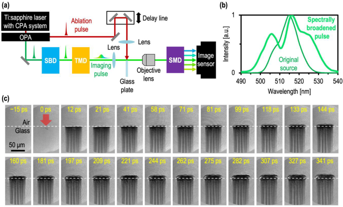
Demonstration of ultrafast imaging of laser ablation with a Ti:sapphire-based system. (a) Experimental setup. (b) Spectra of the imaging pulse before and after spectral broadening. (c) Imaging results. CPA: chirped pulse amplification; OPA: optical parametric amplifier
The spectra obtained before and after the SBD module were measured using a spectrometer (GREEN-Wave-VIS; StellarNet, US) and are shown in Fig. 6a. It was confirmed that a pulse with a center wavelength of 513 nm and an initial bandwidth of 5 nm broadened to 9 nm. The pulse energy before the SBD module was 45 µJ. Next, we captured the images of each spectrally separated pulse on the image sensor after passing through the SMD with and without the CaF2 plate in the SBD, that is, with and without spectral broadening. Figure 6b and c show the captured images with normalized intensities. Spectral broadening effectively reduces the intensity variation between frames. For a more quantitative comparison, the average intensities of the 24 frames acquired for each case, with and without spectral broadening, were normalized, as shown in Fig. 6d. Without spectral broadening, only 12 frames exhibited an intensity exceeding 20% of the maximum intensity, whereas 19 frames met this condition with spectral broadening. Additionally, the intensity exceeded 1% of the maximum intensity in all frames with only spectral broadening.
These results suggest that the developed STAMP system, which incorporates thin-plate-based spectral broadening, is a highly promising tool for ultrafast imaging in narrow-bandwidth Yb-based laser ablation systems. Further spectral broadening by increasing the number of thin plates is effective for increasing the number of frames and reducing the intensity variation between frames.
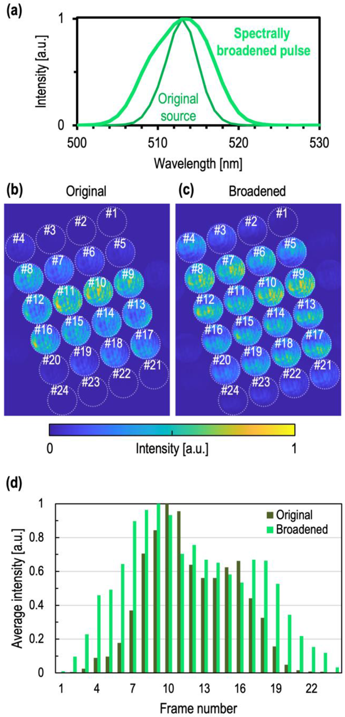
Integration into a pump-probe system using a Yb:KGW laser. (a) Spectra before and after spectral broadening. Acquired image (b) without and (c) with broadening. (d) Normalized average intensity in each frame of the acquired images with and without broadening
4 Conclusion
In this study, we developed a compact STAMP system by introducing thin-plate-based spectral broadening and packaging of the SBD, TMD, and SMD into independent modules. To achieve this, we introduced thin-plate-based spectral broadening as a compact SBD that offers superior stability compared with other methods. For the TMD, we developed a system capable of switching between a grating-pair configuration for picosecond timescales and a spectrum-shuttle configuration for nanosecond timescales, enabling flexible adjustment across a broad timescale range within a single device. For the SMD, we selected a spectral filtering system because of its simple setup with fewer optical elements and its ability to achieve a high spatial resolution.
Using these compact and efficient optical systems, we successfully packaged the STAMP system into three independent modules. This advancement addresses the limitations of existing STAMP systems, which rely on broadband Ti:sapphire lasers and large-scale optical setups, by enabling seamless integration with narrow-bandwidth laser sources. The compact design facilitates easy incorporation into various laser ablation setups, enabling seamless replacement in pump-probe systems. This capability was demonstrated by successfully integrating the developed STAMP modules into a pump-probe system using a narrow-bandwidth Yb-based laser source. Additionally, the effectiveness of the STAMP modules was demonstrated using a Ti:sapphire-based system in terms of ultrafast imaging of laser ablation dynamics.
The compatibility of this STAMP system with different laser ablation platforms opens new possibilities for research and practical applications across fields such as material processing, medical technologies, and the study of laser-matter interactions. The developed system is expected to contribute to the broader adoption of ultrafast imaging and enhance our understanding of diverse ultrafast phenomena.